
This is Part 1 of a Three Part Series
• Chip Resistors Part 1: The Basics
• Chip Resistors Part 2: Types
• Chip Resistors Part 3: Applications and Considerations
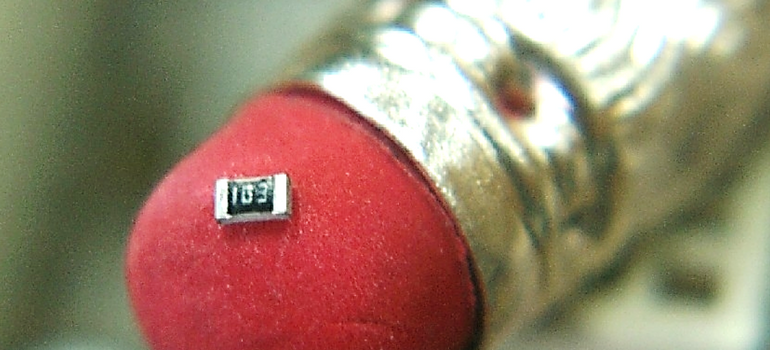
Greetings designers, let’s talk about resistors. Resistors impede current flow, both alternating and direct currents are impeded equally by perfect resistors. The unit for resistance is Ohms (Ω), named after German physicist Georg Ohm. An Ohm is defined as the amount of resistance required to create a voltage drop of 1 volt (V), when the current flow is 1 Ampere (A). From a dimensional standpoint, an Ohm is defined as
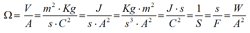
m is meter
- Kg is Kilogram
- s is second
- C is Coulomb
- J is Joule
- S is Siemens
- F is Farad
- W is Watt
…whew! Thanks Wikipedia! ;-)
This is interesting as the Ohm may be described in many different terms including time, distance, mass, charge, energy, capacitance and power…oh yes and conductance (Siemens-1), quite a versatile unit indeed!
Resistance Defined
Now that we understand what Ohms are, let’s find out how resistance (R) is determined. As shown in the figure below, the resistance to a current flowing between plane 1 and plane 2 is found by the relation
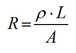
- This is bulk resistance, and the above relation can be further simplified if the conductor is broken into square segments (i.e., if W = L) as shown below. In that case, resistance simplifies to ρ is the resistivity of the material through which the current traverses (units Ω-m)
- L is the length that the current traverses between planes 1 and 2 (units m)
- A is the cross-sectional area of the conductor through which the current traverses (the area of either plane 1 or plane 2 (units m2)
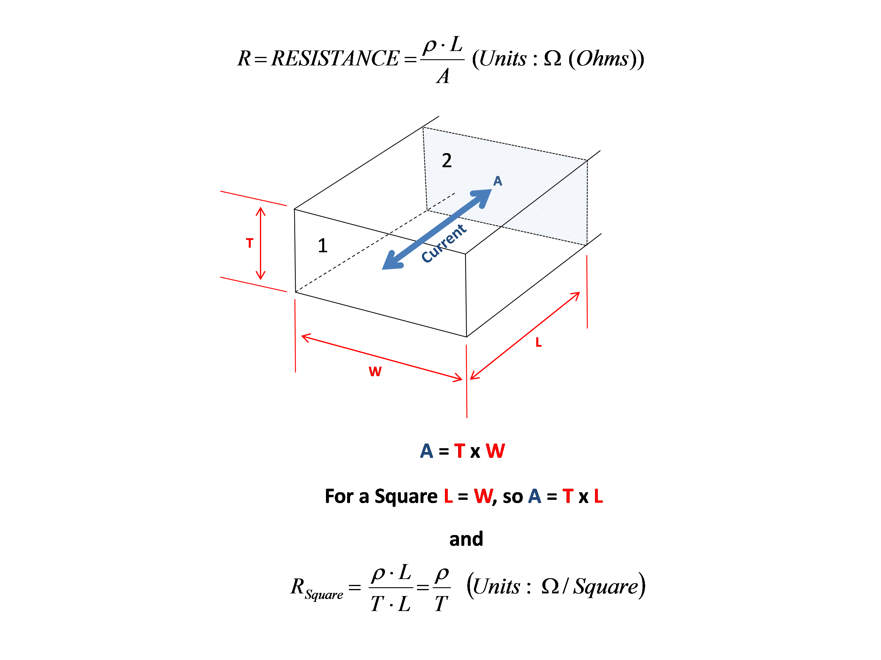
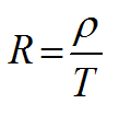
- T is the thickness of the conductor through which the current traverses (units m)
In the above case, resistance simplifies to a value having units of Ohms per square (Ω/□), which is typically called “sheet resistance.” Sheet resistance is a simplification of resistance and is useful to designers as it simplifies the process of resistor design.
Chip Resistor Design
The device designed will typically have at least one resistor element. The element is constant in thickness (T) with a geometry that is comprised of squares. The width and thickness of the trace helps establish power rating as well as the number of squares possible in the trace for a given package size. Thicker and wider squares typically result in the ability to carry more current and to handle more power, but the number of squares (and the resulting resistance per unit length) is reduced. The designer will pick a material with a specific Ω/□ value in order to enable the design to achieve the intended nominal resistance. Further, in order to maximize the number of squares per unit area, a serpentine pattern of interconnected squares is generally used so that more resistance can be packed into a smaller area, making the best of circuit board “real estate.” An example is shown below. In this case, use of a serpentine pattern of squares enables almost 2X the resistance in the same lineal distance.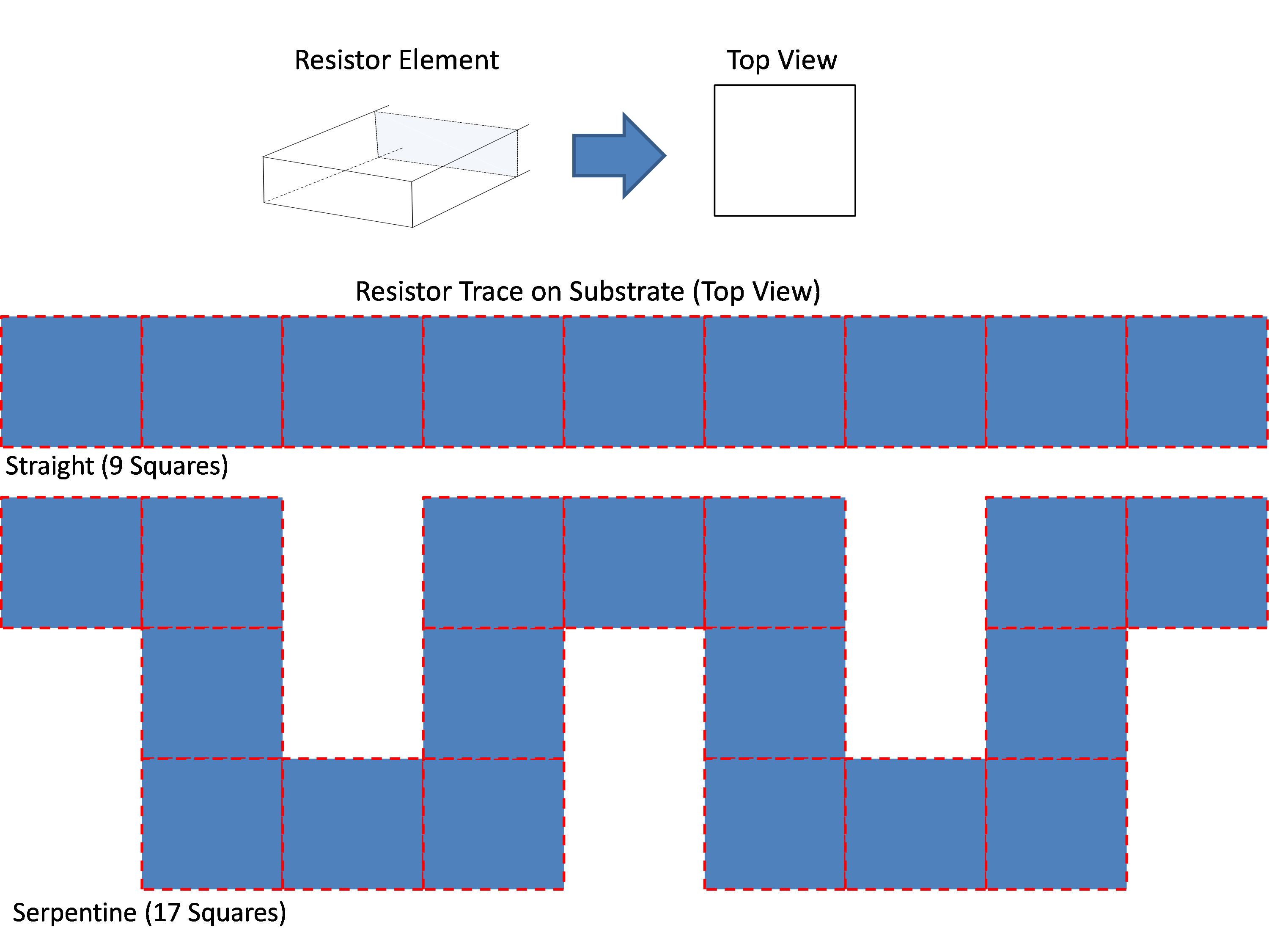
The resistor pattern is deposited on to a substrate, typically comprised of an alumina-based ceramic. However, other materials, such as silicon carbide, etc., may be used for high power applications or other applications. The resistor pattern is connected to two terminals, typically one on each end of the device, in order to enable connection with the circuit board. The resistor trace is then trimmed to meet nominal resistance as necessary, and the resistor trace is over-coated, marked and tested to create the finished product. The resistor device is then connected to the circuit at the assembly facility via surface mount technology (SMT).
Thick and Thin Film Resistors
As mentioned in Chris Gutierrez’s recent blog post, the resistor pattern is typically established via one of two methods, so chip resistors are usually categorized as either thick film or thin film resistors based upon the deposition method used. Chris’ post is an excellent discussion of the two technologies. Additionally, thick film resistor technology benefits from relatively easy composition modification as modification of the resistor thick film “ink” (e.g., chemistry, glass content, dopants for TCR, etc. for the resistor trace) is easily accomplished, whereas it is relatively difficult to change the resistor composition using thin film technology. Thick film resistor materials are generally based upon ruthenium oxide (RuO2) mixed with specialized glass formulations and other dopants to achieved desired properties during firing, while thin film resistors are generally based upon vapor deposited Nichrome and need not fired to achieve desired properties. In contrast, thin film technology typically benefits from better deposit uniformity and more accurate patterning, so both have their advantages.
How They Are Made
The general resistor manufacturing process involves designing the device to fit resistance nominal and power rating in the package size of interest as described above. Next, the resistor material is deposited on the substrate which is selected for mechanical strength as well as electrical and thermal properties. The resistor element deposition is patterned, then adjusted to nominal, then over-coated and the individual resistor chips are singulated, then terminated, tested and packaged. In the case of thick film resistors, the resistor trace chemistry is carefully selected to set Ω/□ as well as to adjust temperature coefficient of resistance (TCR) and other key properties, and the material is deposited and patterned in one step using screen or stencil printing. The thick film resistor deposit is then thermal treated to achieve the electrical properties desired. In the case of thin film resistors, the resistor material is first deposited to achieve a highly uniform thin film, and then patterned using photolithographic technics. In the case of both technologies, the deposit thickness is carefully controlled to achieve the desired Ω/□, and the pattern is adjusted, typically via LASER ablation, to achieve the desired resistance (nominal). The resistor pattern may also be adjusted for high voltage applications, or other specialized applications. The thickness and the pattern uniformity of thick film resistor elements is typically much thicker and less uniform for thick film resistors in comparison to thin film resistors, making thin film resistors more desirable for certain applications (e.g., those involving, precision tolerances, high frequencies or the like).
I hope that you found this useful…TTFN!


