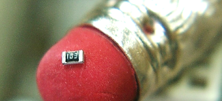
Celebrating 30 years.

Resource Center

Articles, datasheets, technical data, cross reference guides and more. All in one place.

Articles

Tin Whiskers and Chip Components

Posted by Mike Randall on December 23, 2016

26

 What are Whiskers?
“Whiskers” are protrusions that grow from a metal film over time.  They can achieve high aspect ratios, growing to considerable lengths and may result in electrical interconnection of adjacent terminals.  This can happen when a whisker grows from one terminal to another, as in the case of fine pitch electronics, or when a whisker grows, then shears from its source and lands between two terminals interconnecting them electrically.  While this is rare, it has caused considerable concern in the electronics community.

Sn Whiskers
Tin whiskers are Sn protrusions that grow from a tin film.  They may occur on the terminals of chip components such as multilayer ceramic capacitors (MLCCs), chip resistors, chip inductors, varistors, etc.  They are observed much less frequently than in the past as Sn finishes have evolved as manufacturers’ knowledge of Sn whiskers and how to avoid them has developed.  

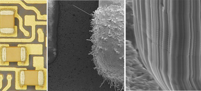
The micrographs above illustrate Sn whiskers at three different magnifications.  At lower magnification (left), they may appear as “fuzz” on the surface of the terminations.  At increased magnification (center), they may present as high aspect ratio protrusions or “whiskers” that grow over time.  At high magnification (right), they typically appear striated on the exterior.  Some of the striae may also have horizontal ridges which have been associated with thermal cycling or other episodic events resulting in whisker growth. 

How They Form
Formation of Sn whiskers is related to stress (usually compressive stress) within the film from which they propagate.  Stress can be caused by several different sources, such as residual stress from the film deposition process (typically electroplating), or from the growth of intermetallic (IMC) phases below the surface of the film as described in a previous post on this blog, or by thermal cycling, or by bending stress in plated leads in the case of leaded components, or the like.  These stresses act to extrude the whiskers out from the plated film.  Subsequently, much effort has been expended in learning how to reduce or eliminate these film stresses in electroplated Sn films.

Where They Occur
Sn whiskers associated with reflow mounted or wave solder mounted chip components are rare because the stresses formed in the electroplated tin film during the plating process are relieved during the soldering process.  They are more common when the mounting technique used does not provide an opportunity for stress relief, such as when mounting with conductive epoxy, and conductive epoxy mounting is mainly where Sn whiskers have been observed in relation to surface mounted chip components.

Sn whiskers have also been observed in unmounted chip components.  This was more prevalent in the early days of conversion from Pb/Sn finishes to Sn finishes for RoHS, but is much less frequent in contemporary chip components as manufacturers have developed low stress Sn finishes through the development of low stress tin electroplating chemistries and processes.  These electrodeposited film chemistries are typically low in carbon and other impurities, such as Zn, and are “matte” in appearance due to relatively large and uniform Sn grain size (typically ~5 µm on average).  With these developments suppliers have been successful in eliminating the incidence of harmful Sn whiskers.  

Solutions and Conclusion
Through development of low stress plated Sn finishes, the worry of Sn whiskers has been eliminated with regard to chip components, if you use a supplier who has conquered plated film stress.  Sn whiskers will also not likely be an issue if you use a solder reflow process or wave soldering to mount your chip components.  If you use conductive epoxy mounting and you still observe Sn whiskers, you may want to heat treat the chip components using a mild heat treatment near the melting point of Sn (~232C).  Use of conformal coating on assemblies will also eliminate whisker-related problems.  I hope that helps.  May you never see another Sn whisker in your assemblies…TTFN!     ;  )   

* Micrographs courtesy of NASA 


Tags: inductor, Resistor, RoHS

The Chip Resistors Part 1: The Basics

Posted by Mike Randall on October 21, 2014

24

This is Part 1 of a Three Part Series

• Chip Resistors Part 1:  The Basics
• Chip Resistors Part 2:  Types
• Chip Resistors Part 3:  Applications and Considerations

Greetings designers, let’s talk about resistors.  Resistors impede current flow, both alternating and direct currents are impeded equally by perfect resistors.  The unit for resistance is Ohms (Ω), named after German physicist Georg Ohm.  An Ohm is defined as the amount of resistance required to create a voltage drop of 1 volt (V), when the current flow is 1 Ampere (A).  From a dimensional standpoint, an Ohm is defined as 

resistors-part-1---graph-1
m is meter 
  • Kg is Kilogram
  • s is second
  • C is Coulomb
  • J is Joule
  • S is Siemens
  • F is Farad
  • W is Watt


…whew!  Thanks Wikipedia!   ;-)

This is interesting as the Ohm may be described in many different terms including time, distance, mass, charge, energy, capacitance and power…oh yes and conductance (Siemens-1), quite a versatile unit indeed!

Resistance Defined
Now that we understand what Ohms are, let’s find out how resistance (R) is determined.  As shown in the figure below, the resistance to a current flowing between plane 1 and plane 2 is found by the relation

resistors-part-1---graph-2

  • This is bulk resistance, and the above relation can be further simplified if the conductor is broken into square segments (i.e., if W = L) as shown below.   In that case, resistance simplifies to ρ is the resistivity of the material through which the current traverses (units Ω-m)
  • L is the length that the current traverses between planes 1 and 2 (units m)
  • A is the cross-sectional area of the conductor through which the current traverses (the area of either plane 1 or plane 2 (units m2)


    resistors-part-1-2
resistors-part-1---graph-3
  • T is the thickness of the conductor through which the current traverses (units m)

In the above case, resistance simplifies to a value having units of Ohms per square (Ω/□), which is typically called “sheet resistance.”  Sheet resistance is a simplification of resistance and is useful to designers as it simplifies the process of resistor design.  

Chip Resistor Design
The device designed will typically have at least one resistor element.  The element is constant in thickness (T) with a geometry that is comprised of squares.  The width and thickness of the trace helps establish power rating as well as the number of squares possible in the trace for a given package size.  Thicker and wider squares typically result in the ability to carry more current and to handle more power, but the number of squares (and the resulting resistance per unit length) is reduced.  The designer will pick a material with a specific Ω/□ value in order to enable the design to achieve the intended nominal resistance. Further, in order to maximize the number of squares per unit area, a serpentine pattern of interconnected squares is generally used so that more resistance can be packed into a smaller area, making the best of circuit board “real estate.”  An example is shown below.  In this case, use of a serpentine pattern of squares enables almost 2X the resistance in the same lineal distance.
resistors-part-1-3

 The resistor pattern is deposited on to a substrate, typically comprised of an alumina-based ceramic.  However, other materials, such as silicon carbide, etc., may be used for high power applications or other applications.  The resistor pattern is connected to two terminals, typically one on each end of the device, in order to enable connection with the circuit board.  The resistor trace is then trimmed to meet nominal resistance as necessary, and the resistor trace is over-coated, marked and tested to create the finished product.  The resistor device is then connected to the circuit at the assembly facility via surface mount technology (SMT).

Thick and Thin Film Resistors
As mentioned in Chris Gutierrez’s recent blog post, the resistor pattern is typically established via one of two methods, so chip resistors are usually categorized as either thick film or thin film resistors based upon the deposition method used.   Chris’ post is an excellent discussion of the two technologies.  Additionally, thick film resistor technology benefits from relatively easy composition modification as modification of the resistor thick film “ink” (e.g., chemistry, glass content, dopants for TCR, etc. for the resistor trace) is easily accomplished, whereas it is relatively difficult to change the resistor composition using thin film technology.  Thick film resistor materials are generally based upon ruthenium oxide (RuO2) mixed with specialized glass formulations and other dopants to achieved desired properties during firing, while thin film resistors are generally based upon vapor deposited Nichrome and need not fired to achieve desired properties.  In contrast, thin film technology typically benefits from better deposit uniformity and more accurate patterning, so both have their advantages.

How They Are Made
The general resistor manufacturing process involves designing the device to fit resistance nominal and power rating in the package size of interest as described above.  Next, the resistor material is deposited on the substrate which is selected for mechanical strength as well as electrical and thermal properties.  The resistor element deposition is patterned, then adjusted to nominal, then over-coated and the individual resistor chips are singulated, then terminated, tested and packaged.  In the case of thick film resistors, the resistor trace chemistry is carefully selected to set Ω/□ as well as to adjust temperature coefficient of resistance (TCR) and other key properties, and the material is deposited and patterned in one step using screen or stencil printing.  The thick film resistor deposit is then thermal treated to achieve the electrical properties desired.  In the case of thin film resistors, the resistor material is first deposited to achieve a highly uniform thin film, and then patterned using photolithographic technics.  In the case of both technologies, the deposit thickness is carefully controlled to achieve the desired Ω/□, and the pattern is adjusted, typically via LASER ablation, to achieve the desired resistance (nominal).  The resistor pattern may also be adjusted for high voltage applications, or other specialized applications.  The thickness and the pattern uniformity of thick film resistor elements is typically much thicker and less uniform for thick film resistors in comparison to thin film resistors, making thin film resistors more desirable for certain applications (e.g., those involving, precision tolerances, high frequencies or the like).  

I hope that you found this useful…TTFN! 

Tags: Thin Film, Thick Film, Resistor, tcr, chip resistor

Venkel's New "Green" RoHS 6/6 Resistor

Posted by Nathan Bailey on September 16, 2014

27

Venkel Ltd. just released the new CRG – RoHS 6/6 “Green” resistor new product offering this month on September 3rd, 2014.  This new resistor series is a general purpose Thick Film Resistor.  It incorporates new construction materials whereby Lead in the glass and Lead Oxide in the resistive element is now eliminated.  The glass frit contained within the resistive element (RuO2) no longer contains any Lead or Lead oxide and will meet the RoHS 1000ppm or 0.1% threshold without taking the 7C-I exemption. 

This product is being produced and released in the industry due to the fact the 7C-I exemption will be expiring on approximately July 1, 2016. (There is a chance the 7C-I exemption could be delayed if enough companies request an extension and an extension is approved by the EU).
A new product data sheet along with material declarations and reliability data are now available on-line at www.venkel.com.  SGS or Interek material reporting validation data (verifying all the material compositions or MDS’s) will be forthcoming within the coming months and available by the end of the year.  Besides the material differences, there are differences in the resistance ranges and in the Temperature Coefficient of Resistance (TCR) when compared to Venkel’s CR series General Purpose Thick Film Resistors.  In some cases, depending on the size and value needed, the TCR may be higher.   The wattage ratings are considered industry standard such as the 0402 and 0603 which are rated at 1/16th Watt (0.0625W) and 1/10th Watt (0.10W) respectively. 
Although the exemption is not set to expire until July of 2016, numerous customers have requested that we have a complaint alternative available now.  Depending on each company’s situation, some must have a strategy in place in order to get new products tested, verified and released.  Many companies want to get ahead of the game on this mandate so no bottlenecks or delays will occur prior to or after the deadline. 
The new CRG series resistors are available now. This series enables you to have your products fully RoHS 6/6 (if that specific resistor product line was the only commodity preventing you from being fully RoHS 6/6 compliant). Please let us know if you have any questions regarding this new product release and if samples are needed for qualification purposes and we will do our best to accommodate you
 
Sincerely,
Nathan Bailey
 

Tags: CRG, Resistor, RoHS, thick, film, CR, RoHS 6/6

Thick Film vs. Thin Film Resistors

Posted by Chris Gutierrez on July 24, 2014

25

What’s the difference between Thin Film Resistors and Thick Film?

When looking at these two types of resistors side by side, they may appear to be similar. The main differences of these two products are the construction, thickness, and application usage of the resistive element itself (hence the descriptions of “thick” and “thin” film resistors). Thick film resistive elements are typically 10 ~ 50 uM in thickness, while thin films are 10 to 200 nM in thickness.  Thick films are applied using a very simple screening process while thin films use a much more sophisticated vacuum process technique that applies the element on a molecular level. Let’s take a look this in detail.

1. Construction

The base material of a thick film resistor element is a Ruthenium Oxide (RuO₂) paste that is screened onto a ceramic substrate.  After this process, the thick film resistors are then fired causing these layers to become glass-like which helps protect the resistive film and makes them less susceptible to failures due to the infiltration of moisture and other contaminants.  Thick film resistor processes can be referred to as an additive process; this means that it consists of layers (resistive element, protective coating, and electroplated terminations) added to the substrate. The thin film resistor element consists of a combination of nickel and chromium (also known as Nichrome) that is applied to a ceramic substrate using a high-voltage, vacuum sputtering process.  A serpentine pattern is then etched into the Ni/Cr element using a photolithographic process. An epoxy layer is screened onto the element to protect it from moisture and other contaminants. This thin film process can be referred to as a subtractive process, meaning unwanted material being etched away in the photo etching process.

2. Thickness
Both thick film and thin film resistors are laser trimmed to their final resistance value. But in general, thin films overall thickness is literally thinner because of the subtractive process. Keep in mind that thick and thin film resistors are also application specific. That is, the application and circuit design will determine what type of resistor is utilized. Thick film resistors are ideal for low cost, economical applications and are also better suited for higher power and high ohmic value requirements. Thin film resistors, on the other hand, offer tighter tolerances for precision applications.

3. Applications
Thin Film v. Thick Film Resistors

Tags: Thin Film, Thick Film, Resistor

Deviant Behavior Part 1: CRLZ Gone Wild

Posted by Mike Randall on June 09, 2014

12

Hey circuit designers!  Have you ever wondered why a circuit that you designed just didn’t act like you thought it should?  Well, that could be due to many reasons; several of which may be related to the capacitors that you selected for your circuit.  In this case you could be a victim of “deviant behavior”…behavior that differs from a norm or from accepted standards.  In this case, the standards of interest would be those set by the mythical “perfect capacitor”…the Unicorn of passive electronics. 

An Imperfect World

You see, like all electronic components, capacitors are not perfect.  The type of capacitor that you select will determine how far from perfection, or deviant the capacitor’s performance will be in your application.  Each real capacitor is a device that has not only a characteristic capacitance (C), but a characteristic resistance (R, typically termed equivalent series resistance or ESR) and an inductance (L, typically termed equivalent series inductance or ESL).  These “parasitics” can adversely affect circuit performance, but in certain situations may be used to your advantage. 

I remember how one of my sarcastic coworkers used to joke about “parasitics.”  He would say, “Shoot!  I don’t understand why our customers are so unhappy about parasitics; we ship them a free inductor and a free resistor with every capacitor!” J

Curves Ahead

Simply put, parasitics affect impedance (Z) as frequency is changed (i.e., the “Z curve”), which may affect circuit performance.  A perfect capacitor exhibits Z = 1/(2πfC) where f is frequency.  As C is increased, Z is reduced in a manner that is linear on a log-log scale (see left side of graphic above).  As f increases, Z of a perfect capacitor continues to decrease in this manner out to infinite frequency.  With a real capacitor, however, C “runs into” either R (typically ESR) or L (ESL) as f is increased, establishing either a “flat” or a minimum in the impedance curve.  If ESR is relatively low, L will largely determine this minimum and the Z curve will be V or gull wing shaped in the case of extremely low ESR.  If ESR is relatively high, R will establish a “floor” or “flat” in the Z curve over a relatively broad range of f.  At higher frequencies L dominates, as Z is ~2πfL, resulting in increasing Z as f is increased in a manner that is linear on a log-log scale (see right side of graphic above).   

You Got to Know When to Hold’em…and Know When to Fold’em

Prudent selection of capacitor type may be useful in achieving a desirable Z curve for your application.  For example, use of capacitors having moderate or high ESR, combined with low ESL, typically results in a relatively flat Z curve.  This may be useful for power delivery designs such as power delivery networks (PDNs), as a relatively “flat” impedance curve is often desirable.  Capacitors, such as controlled ESR reverse geometry or controlled ESR interdigitated capacitors (IDCs) or face down solid electrolyte tantalum (Ta) or low ESL solid electrolyte aluminum (Al) capacitors may be useful in these applications.  On the other hand, use of capacitors having very low ESR combined with low L, may be useful for inline high pass filter designs or for designs requiring high speed decoupling.  Discoidal ceramic capacitors are typically used for high pass filtering, and standard IDC or reverse geometry capacitors may be useful in filtering or high speed decoupling applications.   More recently the design community has favored use of numerous, small case size MLCC in parallel for high speed decoupling designs, as these MLCCs have moderate-to-low ESL (L), take up little space and can be used local to the decoupled device, and are relatively inexpensive.  Additionally, use of capacitors having very low ESR, combined with moderate-to-high L, may be useful in band pass filter designs. Standard MLCCs typically “fit the bill” here, and low loss (high Q), tight tolerance, type 1 dielectric capacitors such as C0G MLCC are typically used here for consistency in resonance frequency (the frequency at which C and L cross if R is 0 or is nearly 0).

A Little Help from Your Friends

Capacitor manufacturers spend significant development resources optimizing the above qualities for different applications.  With regard to parasitics, it’s all about the design, the dielectrics and the electrodes.  For example, in order to minimize ESR, MLCC developers will take advantage of high active layer counts and relatively thick electrodes.  To maximize ESR in an MLCC, special electrode designs may be used in IDC MLCC or resistors may be put in series with other MLCC using specialized termination materials or the like.   For low ESR, special low resistivity internal electrode materials, such as copper or specialized electrode designs may be used. 

Get Real

All combined, these materials and design factors may be used alone, or in combination, to optimize the C, R and L properties of a given capacitor design for one or more specific application(s) requiring a characteristic impedance (Z) curve, making it important for circuit designers to model their circuits with the real (C, R, L and Z) properties of the capacitors selected for their designs.  That way, you may be able to take advantage of that free resistor and inductor that is included with each capacitor! J (At the very least you will be able to compensate for their idiosyncraZies in your design).  Next time we will discuss part 2 of Deviant Behavior, but as Winnie the Pooh would say, “Ta ta for now!” (TTFN :-)) 

Tags: inductor, Resistor, capacitor, high-q

Subscribe to Resource Center Updates