Celebrating 30 years.

Resource Center

Articles, datasheets, technical data, cross reference guides and more. All in one place.

Articles

Chip Resistor Power Considerations

Posted by Mike Randall on December 02, 2014

3

Seasons’ greetings designers!  Chip resistors are important components in many circuit designs.  By their very nature, resistors turn the flow of electricity into heat.  They can dissipate considerable power as heat depending upon the design in which they are utilized. 

Background

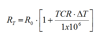
Resistors reduce voltage within a circuit, turning said voltage reduction into heat via Joule heating following the relation:

                    where:

  •                                              P = power (W)
  •                                              I = current (A)
  •                                              V = Voltage (V)
  •                                              R = Resistance (Ω)


The creation of heat via resistive or Joule heating occurs within the resistor element of the device, causing it to heat up as it passes current.  Some of the heat generated escapes from the resistor element to the outer environment, through the components of the chip resistor.  Heat dissipation can only happen so fast however, and the amount of heat that is retained within the device heats it to higher temperature.  The amount that the temperature increases is typically simplified to a linear value that is specified for the device.  This value is typically stated in oC/W (degrees Celsius per Watt of power dissipated by the resistor element), and the nominal power rating of the chip resistor is determined from that value, amongst other considerations.  The nominal power rating of a chip resistor is given in Watts.  The value is determined by calculation based upon experimentation and is typically verified through reliability testing of several batches of qualification devices.

Further, the nominal power rating of the chip resistor decreases once the operating temperature of the device exceeds a given temperature (typically 70oC).  In this case, the nominal power rating of the chip resistor is reduced at a rate of ~-1.2%/oC as the device temperature increases past 70oC, as indicated in the illustration below, and the chip resistor is completely derated by 155oC (the maximum use temperature).  It may also be possible to increase the rating of the chip resistor selected if the operating temperature of the chip resistor is always kept below 70oC using an extrapolation of the derating line in the figure below to temperatures less than 70oC (e.g., ~+1.2%/oC below 70oC), but be sure to get your supplier’s “blessing” before you do this, as this practice may result in warranty issues regardless of whether or not it is appropriate.

Improper chip resistor selection with respect to power rating may result in aging (embrittlement) or even melting of solder joints, which will lead to a lack of reliability of the chip’s solder joints.  It can also result in a loss in printed circuit board (PCB) performance, or even failure of the PCB.  Improper component selection or circuit design can also result in poor chip resistor performance, such as high drift in resistance value, or the like.  These effects may not be reversible without reworking or even replacing the component.

Considerations

For proper design, the circuit designer needs to carefully consider the balance between component selection and thermal management considerations in order to achieve a thermal equilibrium condition in the device that does not significantly exceed the operating temperature of the circuit.  Heat generated during operation must be removed from the device in an efficient manner.  We know that heat may be removed via one or more of the mechanisms of conduction, convection or radiation.  However, in our case, radiation and convection are typically minor contributors to heat flux as the temperature is too low to have significant radiation, and the ambient is typically a poor convective medium.  So we must rely on conduction for removal of the large majority of the heat generated.  The primary path for removal of the heat generated is the conduction path of heat through the metal terminals of the chip resistor, to the conductive traces of the PCB and out into the thermal mass of the PCB.  This heat flow can be maximized in the design of the chip resistor by maximizing the size of the terminals (i.e., using a large case size chip resistor) or through the use of larger solder connections, or through the use of two sided metallization and/or thicker metallization on the PCB, either alone or in combination with the use of prudently placed thermal vias in the vicinity of the mounting pads.  Each of these methods, especially when used in combination, results in an improved thermal conduction path for heat from the chip resistor. 

Further, material selection is important.  For example, the thermal conductivity (KTh) of alumina, the material typically used for chip resistor substrates is ~24-30 W/mK.  Use of more exotic electrically insulating materials for the chip resistor substrate, such as Silicon Carbide (KTh ~350-500 W/mK) or even diamond (KTh ~900-3,000 W/mK), helps to increase the power rating of the device by providing a greater dissipation path for heat generated in the resistor element.  However, this can be highly expensive, and it is important to balance the improvement in thermal performance with the cost of utilizing exotic materials.  In the case of diamond, for instance, the increase in cost is usually prohibitive.  The above discussion also applies to the over-coating material and to the terminal materials.  Additionally, thermally conducting, but electrically insulating materials, such as thermally conductive epoxies or the like, may be used to underfill the chip resistor in order to enhance thermal conduction from the bottom of the chip resistor into the PCB.  Thermal vias below said underfill can further enhance conduction of heat from the chip resistor to the PCB as well.   

Summary

It is important to consider power rating when selecting a chip resistor for your circuit design.  While it may be tempting to use the smallest chip resistor possible, that may not be prudent as it may lead to overheating.  As the balance between heat generation and heat dissipation is paramount, it is important to select the appropriate chip resistor as well as to properly design your PCB, making sure to use the appropriate amount of metal in the traces and lands, as well as thermal vias, etc. where prudent.  The balance between power dissipation and cost is an important consideration as well, since use of high thermal conductivity materials and specialized designs and cooling schemes, etc. can quickly become prohibitively expensive. 

High power chip resistors are designed using economical high thermal conductivity materials, combined with resistor patterns having better thermal properties, as well as by utilizing modified construction and processing techniques, all in a cost effective manner.  High power chip resistors may have double the power rating or better compared to the same case size standard chip resistor.  Because of this, they are typically an economic option for the designer when it is important to maximize power density as well as component density within the circuit design.  Additionally, if the designed circuit is kept below 70C, it may be possible to increase the power rating of the chip resistor selected using a slope similar to, or less than the slope of the derating line extrapolated to the operating temperature below 70oC.  However, be sure to talk to your chip resistor supplier, prior to adopting this practice, in order to make sure that this practice does not void any warranties.    I hope that the above helps you when you need to select a chip resistor for your design.  Until next time…TTFN!


Tags: Chip Resistors, High Power Chip Resistors, Resistors

Chip Resistors Part 3: Applications and Considerations

Posted by Mike Randall on November 25, 2014

5

This is Part 3 of a Three Part Series

  • Chip Resistors Part 1: The Basics
  • Chip Resistors Part 2: Types
  • Chip Resistors Part 3: Applications and Considerations

Greetings designers!  In my last post we discussed several types of chip resistors and applications.  In this post, we will discuss some application factors as well as important considerations. 

Applications

Resistors are used in numerous applications, such as current sensing, circuit tuning, voltage dividing, gain setting, high frequency terminations and myriad high voltage and high power applications.  Many of these applications may also be environmentally challenging, such as high temperature, high sulfur or high humidity atmospheres or the like.  This article focuses on the potential effects of precision/matching, frequency, temperature and current as each may be an important factor in your application.

 Precision and Matching

In certain applications, it is highly important to use resistors that are well-matched.  For example in the non-inverting amplifier circuit (Op-Amp based) illustrated below, the gain (G) is established by the ratio of the resistor values shown through the relation G=1+(R2/R).  If a minimum amplifier precision of 1% is required, then the nominal resistance values of resistors R1 and R2 not vary more than +/-0.25%.  Further, it is important that the resistors used in this application have well-matched temperature coefficient of resistance (TCR).

For example, using resistors having TCR of 200 ppm/C would result in 1% change in gain (G) if ΔT between them is 50C.  This could occur as a result of self heating of R2 for instance, or if one of the resistors is placed too close to a heat source (e.g., high power actives or the like).  For high precision systems (say 10 bit, requiring 0.1% G accuracy or better), matching of R1 and R2, combined with use of low TCR (and similar TCR) resistor materials becomes important.  Additionally, design that minimizes ΔT between R1 and R2 is important.  In these cases, the use of high precision resistors or of matched resistor networks is a common solution.  Trimmable resistors may also be valuable in these applications.

Temperature Considerations

As mentioned above, temperature effects are important for resistors that must be matched, but they are also important in other applications requiring stable resistance.  Low TCR is generally preferred, but must be balanced with the economic factors of your design, as low TCR resistors are generally more expensive.  The effect of TCR on resistance is calculated using the relation:

chip-resistors-3-2

where:

  •      RT is resistance at the temperature of interest (Ω)
  •      R0 is the nominal resistance (Ω)
  •      TCR is temperature coefficient of resistance (PPM/C)
  •      ΔT is the change in temperature from nominal (C),

Indicating that the use of low TCR materials in the resistors that are used in your design is preferred, and that ΔT in your circuit’s operating environment should be kept to a minimum in order to avoid resistance changes in your design.

Additional variation in resistance may result from thermoelectric effects.  Chip resistors typically are made from at least two different conductor materials; the resistive element is generally one material and the external terminal material, or the termination, is generally at least one different conductor material.  When dissimilar metals are joined, a thermocouple may be formed due to the Seebeck effect.  This effect results in the generation of a small voltage between the terminals of the resistor that is based upon the difference in temperature (T) between the terminals.  It is similar to the phenomenon that results in a thermocouple output voltage that makes thermocouples useful for measuring temperature.  This effect can be significant in precision circuits, so it is important to design your circuit such that ΔT between each chip resistor terminal is minimized (e.g., design such that cooling airflow traverses each resistor terminal equally, or design that avoids placement of one terminal near a heat source, or the like). 

Random thermal movement of charge carriers in a resistor element also produces noise that is proportional to the operating temperature, as well as to the use bandwidth, the current and the resistance of the device in a one half power manner.  This can become significant as one or more of operating temperature, current, use bandwidth or resistance is increased.[1]  

Frequency Considerations

Resistor Parasitics

While a resistor is conceptually simple, each has non-ideal characteristics, as no device is perfect.  In the case of a chip resistor, said device will have capacitive and inductive parasitics.  The effect of the capacitance can be modeled as a capacitor in parallel with the resistor, and the effect of inductance as an inductor in series with the resistor.  Parasitic capacitance of chip resistors tends to be quite small (<1 pF), leading to low frequency (near DC) impedance that is generally >100 GΩ, which will have minimal effect on the resistance value of all but the highest resistance value resistors.  This effect is generally compensated during the design process but should be understood as the compensation likely changes with frequency.  With increasing frequency the impedance associated with the parasitic capacitance is reduced.  This effect can be significant when capacitive parasitic impedance is similar to, or less than, the nominal resistance value.  For example, in the case of a parasitic capacitance of 1 pF, the associated capacitive impedance at 100 MHz will be about 100 Ω.  This parasitic could affect the actual impedance by as much as 33% in the case of a 50 Ω termination resistor at 100 MHz.  Again, this is usually compensated in the design, but it is important to understand as the effect changes with frequency and with resistance value.  The inductive parasitic may also be important at high frequencies.  For example, a parasitic inductance as low as 10 nH at 100 MHz will contribute about 50 Ω in to the impedance of the resistor.  Again, this is compensated for during the design process in order to achieve proper performance over a range of frequencies, and thus is important to the understanding of the frequency range appropriate to the device selected for your circuit and your situation, as the combined effect of the parasitics upon overall impedance changes with changing frequency.

Skin Effect

As frequency is increased in an AC circuit, current flows more and more toward the periphery of the conductor through which it flows.  This is called the skin effect, and may result in increased impedance as frequency is increased.  The current density in a conductor (or resistor element) decreases from the outside to the inside of the conductor according to the relation: 

               where:

  •      Jd is the current density at depth d into the conductor (A/m2)
  •      JS is the current density at the surface (s) of the conductor (A/m2)
  •      d is the depth into the conductor (m)

δ is the skin depth of the material comprising the conductor (m) as defined by the relation:

where:

  •      ρ is the resistivity of the conductor or resistor material (Ω-m)
  •      f is frequency (Hz)
  •      µ0 is the magnetic permeability of free space (1.257×10⁻⁶ H/m)
  •      µr is the magnetic permeability of the conductor or resistor material (H/m)

Skin depth tells you the depth at which the effective conductivity of a material is reduced to 1/e (~37%) of its full value at the exterior skin.  As frequency and/or magnetic permeability are increased, skin depth δ decreases at a half power rate, and as resistivity increases, δ increases at a half power rate.  This is important mainly in thick film resistors where the thickness of the resistor element(s) tends to be considerably greater than for thin film analogs, making thick film resistors generally more susceptible to increased impedance at high frequency as compared to thin film resistors due to the skin effect.  Additionally, perimeter geometries of printed thick film resistor traces tend to be less consistent compared to thin film resistor traces, and as the current is forced toward the outer portion of the conductor, the current path becomes more tortuous, further increasing apparent impedance at elevated frequencies in thick film resistors.  Magnetic permeabilities and resistivities of the resistor trace materials are also important considerations. To minimize the skin effect (i.e., to maximize δ), it is generally preferable to use high resistivity, low magnetic permeability materials, and to understand these values at the frequencies and fields of your application as they may change greatly with changing field or frequency.

Summary

Resistors have myriad applications in electronic circuits.  For gain setting, it is important to make sure that precision and TCR are appropriate for your application, and using a resistor network, or precision resistors, or trimmable resistors is appropriate.  Additionally, to avoid temperature-related resistance change, as well as other signal noise related effects, it is important to design for minimal ΔT both between resistor terminals and between individual resistors in your circuit as well as to keep the overall temperature of the resistors as low as practicable.  It is also important to understand how parasitics affect resistor performance as frequency is changed, and to minimize parasitics in a manner that is cost effective for your application through both device selection and circuit design.  For high frequency applications, skin effect may also become important, and the potential geometric advantages of thin film resistors over thick film resistors, as well as the properties of the resistor materials used in the device selected, should be carefully considered.  Until next time…TTFN!

Tags: Thin Film, Resistors, tcr, Thin Film Resistors

Subscribe to Resource Center Updates