Celebrating 30 years.

Resource Center

Articles, datasheets, technical data, cross reference guides and more. All in one place.

Articles

DEMAND DRIVERS FOR PASSIVE COMPONENTS IN 2020

Posted by Anand Venkatrao on January 07, 2020

DOWNLOAD THIS ARTICLE (PDF) 

With 2019 behind us, we would like to provide you with our forward-looking thoughts on new demand drivers for 2020. These eight drivers below do not encompass all the potential demand drivers for passive components. The AR (augmented reality) movement is one to keep an eye on, but rumors out of Magic Leap say they have sold only 6,000 headsets compared to 100,000 the CEO wanted to sell (1). If Apple introduces an AR headset, it will be a gamechanger for this space. 2020 is going to be the year of 5G, and the widespread adoption of Industry 4.0 (4th Industrial Revolution). Here are Venkel’s top eight growth demand drivers for 2020:

Smartphones

Depositphotos_319109994_l-2015

Smartphone demand is still incredibly strong even though the market has reached a saturation point. The upgrade cycle for Android and iOS phones is about to kick in big time with the introduction of 5G phones and improved cameras (i.e. the iPhone 11 Pro with 3 camera sensors). During this year’s Consumer Electronic Show (CES) in Las Vegas, the president of Qualcomm said that there will be over 200 million 5G smartphones sold this year. Also, that he expects that 2020 will be the year that 5G finally scales (13).

Smartphone demand over the next 4 years is expected to average around 1.4 Billion devices sold per year, according to IDC (International Data Corporation) (2). This demand includes Android and iOS devices. This doesn’t consider any tablets. According to our research, the iPhone X has around 1,000 MLCCs (multilayer ceramic capacitors) per device, and an average Android has around 700 MLCCs per device. If we use the projections that IDC has on the amount of Android and iOS devices sold, the smartphone industry roughly consumes around 1 Trillion MLCCs per year! This segment is the largest consumer of MLCCs in the world. When the smartphone industry projects increase or decrease, the ripple effects of this supply shortage or glut can be felt. A 10% fluctuation equates to roughly 100 billion MLCCs. The industry cannot absorb this kind of demand so that is why we see some parts go into allocation or surplus based on this.


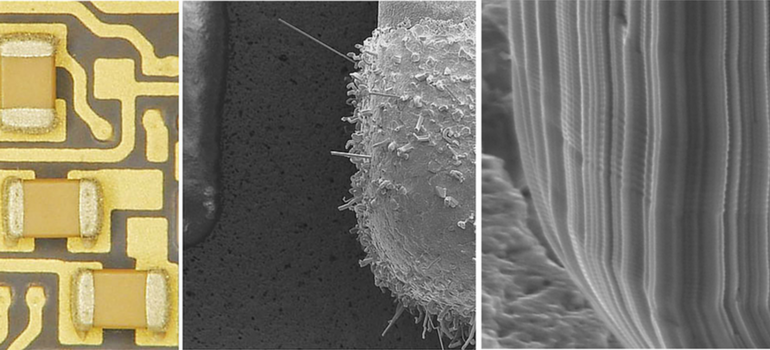
Related Resource

Snapshot - Demand Drivers for Passive Components in 2020

New call-to-action

DOWNLOAD NOW


Artificial Intelligence Accelerators

Depositphotos_215898732_xl-2015

AI Accelerators are specifically designed semiconductors, FPGAs or ASICs that create hardware acceleration for artificial intelligence applications, especially neural networks, machine vision and machine learning. These devices sit inside servers/personal computers via a PCI or are tethered to them via USB. For example, Google advertises that each Accelerator utilizing their Tensor Processor Unit (TPU) can process 1 million photos per second (3).

The AI Accelerator is a relatively new type of hardware that first came into play about three to four years ago with little fanfare. But now, these accelerators are in high demand thanks to the approval/adoptions of the Edge Computing concept. There are now over 45 startups focusing exclusively on these accelerators, either with hardware and/or software. Some like Graphcore and Cerebras have each raised more the $100 million to prove that their technology can be used to better execute AI functions. Hebana, an AI accelerator developer that focused on programmable chips for the data center, just got bought for $2 billion by Intel in mid-December 2019. Intel estimates that the TAM for AI silicon will be greater than $25 billion by 2024 (4).

Google, NVIDIA, AMD, Amazon and the aforementioned Intel are all working on these devices as well. These companies believe that these AI chipsets will give their products and/or services a competitive advantage over their competition.

How does this effect the demand of components going into 2020? In 2016, it was reported that Amazon Web Services had around 1.3 million servers and Google had around 2.5 million servers. If every server is going to get an AI Accelerator, that is at least 3.8 million chip sets alone for just Amazon and Google. Microsoft, NVIDIA, IBM, and Google all have their own Cloud hosting. Not to mention Facebook builds their own hardware/infrastructure as well. All these platforms will benefit from these devices. If each chipset has around 100-200 MLCCs (low estimate given how much computing power and memory these have) and there are 10 million servers that need these chips, that equates to 1-2 billion MLCCs

Automotive – Conventional Combustion Engine Cars and Hybrids

depositphotos_41114019-stock-photo-rear-view-of-luxury-car

The demand for passive components in cars is about to increase exponentially. We are starting to see more electronics in each car that is being produced. All types of cars are getting smarter via the Advanced Driver Assistance Systems (ADAS) and autonomous vehicle adoption. According to Murata, here is a current breakdown of the number of MLCCs and Inductors per car (5):


Conventional Cars (Ford F-150)

Hybrid (Toyota Prius)

Full Electric Vehicle (Tesla)

MLCCs (pcs)

3,000

6,000

10,000

Inductors (pcs)

300

600

600


MLCCs per

Conventional (Ford F-150)

Mild Hybrid (Toyota Camry)

Full Hybrid (Toyota Prius)

Plug-In Hybrid (Chevy Volt)

Battery Hybrid (Tesla)

Powertrain

300 to 500

1,000 to 2,000

1,200 to 1,600

1,500 to 2,000

2,000 to 2,500

ADAS

2,000 to 3,000

Safety

300 to 1,000

Non-Safety

500 to 2,500

Infotainment

500 – 2,500

Source: Murata Information Meeting 2019 (5)

The MLCC count is only going to increase as cars get more advanced. The big trend for cars is going to be the “Connected” Car which will be able to communicate with other cars on the road, the infrastructure (i.e. lights) and with people on the road. Soon, you will be able to get an alert of a speeding car coming down an intersection on your phone that is dependent on your physical location. All these advancements require passive components, especially MLCCs and inductors.

The ADAS boom is already here with the proliferation of backup cameras, tire pressure monitors, remote start, remote diagnostics and blind spot monitors. All of this gadgetry requires more passive components. You can see above that the ADAS components take up a majority of the MLCCs per car, and evidence suggests this number will only increase as more cars slowly start getting some “autonomous” features like self-park and summon (current feature in Tesla’s).

In 2018, there were roughly 80.6 million cars sold worldwide, and in 2019, it is estimated at 77.5 million cars sold. For 2020, the global projection is set to be 78 million cars (6). Even though the number of cars being sold is decreasing, there is a large increase in the amount of electronics per new car. Because of this uptick, we believe the market for automotive MLCCs is going to expand tremendously. Morgan Stanley projects the TAM of all types of MLCCs could increase by 19-28% from 2020 to 2021. This could explain why Murata and TDK have de-emphasized thousands of commercial grade MLCCs and are expanding their automotive lines. The projected MLCC demand based on 78 million cars X 4,000 MLCCs (averaging Conventional with Hybrid) will be roughly 312 billion MLCCs just for 2020.

Electric Vehicles & Electric Bikes

Depositphotos_209513972_xl-2015

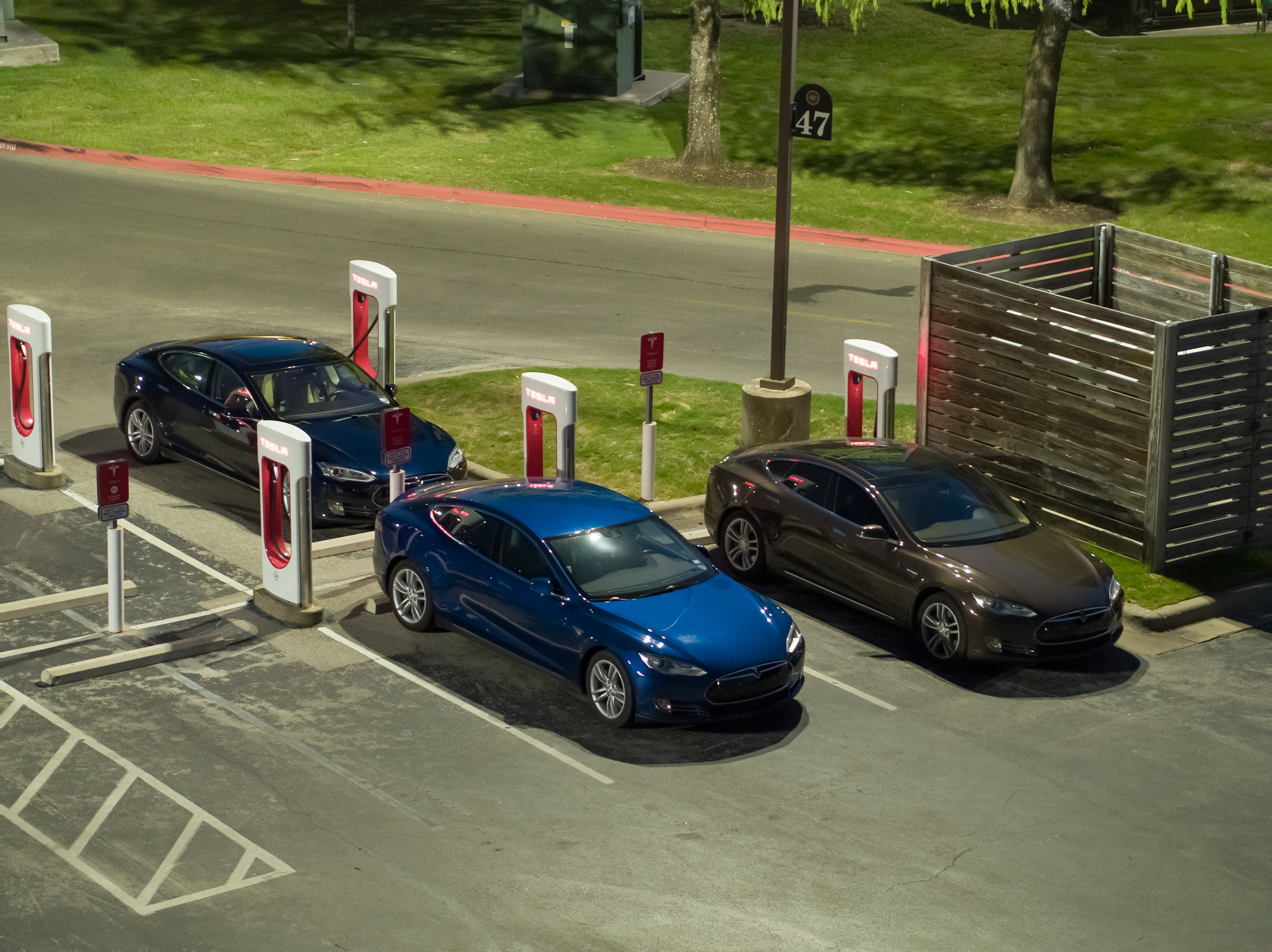
In 2018, there were 1.6 million electric vehicles sold. It is projected that number will go up to 12 million EVs sold per year by 2025, according to Deloitte (7). If each EV averages around 10,000 MLCCs, that will be roughly 120 billion MLCCs per year alone on EVs, by 2025.

Electric bikes or e-bikes are expected to be in high demand due to massive market penetration in Asia and Europe. In 2013, there were 32 million e-bikes sold throughout the world. Between now and 2023, Deloitte is projecting there are going to be 130 million bikes sold! E-bikes, unlike EVs, do not require any specialized plug or in home system. These can be charged via a typical wall outlet. The demand for these are increasing as more and more people around the world relocate into modern cities. The largest shift in populations moving is occurring in Asia. There isn’t much room for more cars and/or parking lots so people are adopting e-bikes at very high rate. The cost per bike is also going down with the increase in scale and lower cost of lithium batteries. Based upon the Xiaomi MiJia bike 2017 model, each e-bike will have over 55 MLCCs and over 100 resistors. 

Consumer Internet of Things

Depositphotos_199221244_xl-2015

We have finally achieved a mass adoption of the Internet of Things (IoT). We have been hearing about it since 2015, but it has taken time to get the IoT infrastructure in place. By IoT, we mean any device that is connected to the internet or an intranet via wireless or wired connection. Common examples are Google Home, Amazon Alexa, Nest thermostat and smart doorbells. Most of these devices are powered by a SoC (System on Chip). According to our research, most of these devices have around 50 MLCCs per. An Amazon Alexa Dot has over 75 MLCCs per. Amazon has sold more than 100 million devices as of January 2019.

26 billion IoT devices are currently connected in the world. This number is expected to reach 75 billion by 2025 (8). That is roughly 10 billion new IoT devices added each year for the next 5 years. If each device has a similar component count to the Amazon Alexa Dot, IoT could end up consuming 1 trillion MLCCs per year! Smartphone and IoT combined are projected to use over 2 trillion MLCCs per year.

Industrial Automation or Industrial Internet of Things (IIoT)

Depositphotos_210855748_xl-2015

This is being discussed also as Industry 4.0 or the 4th industrial revolution. What does this mean exactly? It is a convergence of big data analytics, high end servers, edge computing, AI, machine to machine (M2M) devices and sensors. The example I like to use is imagine if a large-scale farming operation has over 5,000 acres. Each crop area could have a dozen or so moisture sensors that communicate with a wireless base station. When the moisture drops to a certain level, it kicks of the irrigation system and/or delivers nutrients based on the PH levels. It provides the farmer a higher level of comfort and reduces the physical amount of time someone has to inspect. This system would also be performing real time analysis on crop conditions and weather patterns to ensure efficiencies.

There are factories all over the world already utilizing connected sensors to monitor their process. Rockwell Automation is investing in this space with their FactoryTalk line. These sensors provide a machine operator or plant manager with historical data on how well certain machines or processes are working as well as where/when exactly a fault has occurred.  

Real time analytics are going to get supercharged by 5G and Edge computing in terms of “big data” analyzing large scale operations more efficiently. Companies could start deploying their own 5G small cells, instead of WiFi or ZigBee.

It is too early in the stage to predict MLCC and Resistor consumption, but it will be very significant.

5G Infrastructure/Modems/Backend Equipment

Depositphotos_217589800_xl-2015

The build out of the 5G infrastructure is going to be the catalyst for smartphone demand, IIoT, IoT and Autonomous Vehicles. Without this technology, Industry 4.0 will not be able to operate. This is because with 5G comes increased bandwidth and lower latency. Lower latency is key for the autonomous vehicles ability to communicate with surrounding cars, city infrastructure and sensors to communicate what is a life form. Edge computing will also require the speed of 5G in order to process certain aspects of the autonomous vehicles’ functions.

There is a big difference between 4G LTE and 5G, in terms of base station density. There are about 20-25 per square mile for 4G. Whereas, the 5G base stations there might need to be 100-125 per square mile (9). Also, line of sight is key to achieving the high speeds with 5G. Because of this technological difference, telecom companies will have to install more base stations in a city or rural area. China apparently has already deployed over 100,000 5G base stations during their “testing” period. According to a Politico article (10), the USA will deploy 800,000 base stations by 2026. Based on our research and intelligence, the 5G base station has roughly 15,000 MLCCs and 10,000 resistors per device. This is around a 2-3 times increase over the 4G base station. The reason for this increase is the 5G device is 16 channels by 16 channels, and a 4G base station is 4 channels by 4 channels. You are increasing the bandwidth 4 times.

Imagine each lamppost downtown in your city having a 5G base station on it in order to take advantage of the increased speed of the network. AT&T, Sprint, T-Mobile and Verizon are all deploying their 5G base stations throughout the USA. The base station demand is just starting to ramp up. These base stations have large case size (0805, 1210 and 2220) capacitors as well as high voltage, High-Q NP0 and “popcorn” (0.1uF or less/50V or less) MLCCs. Large case size MLCCs could be impacted by the roll out because manufacturers cannot achieve, for example, a 4.7uF, 100V, X7R in anything smaller than a 1210. Parts like this will always be in demand, do not be concerned that these larger size parts will be obsoleted.

Verizon is the first telecom to offer an in home 5G modem for consumers. It’s offering is packed with features like Amazon Alexa, 10W speaker, Bluetooth playback and Wi-Fi 6 (12). We expect that demand for the in home 5G modem will increase rapidly once the rollout is more widespread. The potential is for each home to have one of these instead of cable or fiber modem. Like everything with 5G, these modems will most likely require more passives to handle the increased bandwidth and power requirements.

With the 5G infrastructure build up comes investment in the network’s back office as well. According to McKinssey, the entire infrastructure of these telecoms must be upgraded in order to effectively deploy 5G to a city or area (11). The industry is going to see demand for 5G base stations, 5G Modems (vehicle, machine to machine (M2M), home or business) and 5G test and measurement equipment. For the most part, everything has to be new in order to take advantage of the speed.

DDR5 Memory Modules

DIMM-DDR5

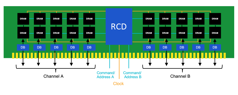
Based on our research, DDR5 will begin to slowly trickle out towards the end of 2020. Adoption rate will be slow at first, but it should ramp up very quickly especially on the server side starting in 2021. Our sources project that DDR5 will require about 10-15% more MLCCs per module. While it won’t affect passive component demand in 2020, we believe DDR5 will be a significant consumer of passive components in 2021 and beyond.

So what does all this mean?

To help put all this information into perspective and to summarize our conclusions, based on our research we believe the total combined annual capacity of all MLCC manufacturers worldwide to be around 4.5 Trillion pieces. In our estimation, just the 8 sectors mentioned above will utilize approximately 3.3 Trillion pieces or roughly 73% of capacity, leaving 27% for everything else!

So, is the industry going to go back to the shortage/allocation days like in 2018? – maybe, but most likely not as bad. That doesn’t mean you shouldn’t be doing things to prepare yourself or your company for what lies ahead. So what does lie ahead? Increased lead times, possible more Not Recommended for New Design (NRND) or End of Life (EOL) parts from the other manufacturers, tightening of availability for popular 5G parts (like the 0402, X7R, 0.1uF), and possibly more delays from IC manufacturers like Intel. Intel is struggling to keep up with demand right now for their chips. If you have the ability, I would recommend adding more sources to the AVL/Bill of Materials in case things really tighten up. If you can take care of something like this now, you don’t have to scramble later when availability tightens up.

Please know that this is our opinion of the 2020 market based on our own research and intelligence.


References:

  1. https://www.theinformation.com/articles/dented-reality-magic-leap-sees-slow-sales-steep-losses
  2. https://www.idc.com/getdoc.jsp?containerId=prUS45115119
  3. https://cloud.google.com/blog/products/ai-machine-learning/cloud-tpu-breaks-scalability-records-for-ai-inference
  4. https://newsroom.intel.com/news-releases/intel-ai-acquisition/#gs.q06r6c
  5. https://www.murata.com/-/media/webrenewal/about/newsroom/news/irnews/irnews/2019/1129/1911_e_speach.ashx?intcid5=com_xxx_xxx_hm_ms1_xxx&la=en-us
  6. https://www.forbes.com/sites/neilwinton/2019/12/05/global-auto-sales-will-slide-again-in-2020-but-china-rally-begins/#580b9efa53fe
  7. https://www2.deloitte.com/content/dam/insights/us/articles/722835_tmt-predictions-2020/DI_TMT-Prediction-2020.pdf
  8. https://ipropertymanagement.com/research/iot-statistics
  9. https://www.newtec.eu/article/article/choosing-the-right-connectivity-for-5g
  10. https://www.politico.com/news/2019/12/29/big-barrier-trump-5g-america-089883
  11. https://www.mckinsey.com/industries/technology-media-and-telecommunications/our-insights/the-road-to-5g-the-inevitable-growth-of-infrastructure-cost
  12. https://www.verizon.com/about/news/verizon-5g-home-internet-coming-chicago
  13. https://www.digitaltrends.com/mobile/5g-qualcomm-ces-fixed-wireless-lenovo/

Tin Whiskers and Chip Components

Posted by Mike Randall on December 23, 2016

26

 What are Whiskers?
“Whiskers” are protrusions that grow from a metal film over time.  They can achieve high aspect ratios, growing to considerable lengths and may result in electrical interconnection of adjacent terminals.  This can happen when a whisker grows from one terminal to another, as in the case of fine pitch electronics, or when a whisker grows, then shears from its source and lands between two terminals interconnecting them electrically.  While this is rare, it has caused considerable concern in the electronics community.

Sn Whiskers
Tin whiskers are Sn protrusions that grow from a tin film.  They may occur on the terminals of chip components such as multilayer ceramic capacitors (MLCCs), chip resistors, chip inductors, varistors, etc.  They are observed much less frequently than in the past as Sn finishes have evolved as manufacturers’ knowledge of Sn whiskers and how to avoid them has developed.  

The micrographs above illustrate Sn whiskers at three different magnifications.  At lower magnification (left), they may appear as “fuzz” on the surface of the terminations.  At increased magnification (center), they may present as high aspect ratio protrusions or “whiskers” that grow over time.  At high magnification (right), they typically appear striated on the exterior.  Some of the striae may also have horizontal ridges which have been associated with thermal cycling or other episodic events resulting in whisker growth. 

How They Form
Formation of Sn whiskers is related to stress (usually compressive stress) within the film from which they propagate.  Stress can be caused by several different sources, such as residual stress from the film deposition process (typically electroplating), or from the growth of intermetallic (IMC) phases below the surface of the film as described in a previous post on this blog, or by thermal cycling, or by bending stress in plated leads in the case of leaded components, or the like.  These stresses act to extrude the whiskers out from the plated film.  Subsequently, much effort has been expended in learning how to reduce or eliminate these film stresses in electroplated Sn films.

Where They Occur
Sn whiskers associated with reflow mounted or wave solder mounted chip components are rare because the stresses formed in the electroplated tin film during the plating process are relieved during the soldering process.  They are more common when the mounting technique used does not provide an opportunity for stress relief, such as when mounting with conductive epoxy, and conductive epoxy mounting is mainly where Sn whiskers have been observed in relation to surface mounted chip components.

Sn whiskers have also been observed in unmounted chip components.  This was more prevalent in the early days of conversion from Pb/Sn finishes to Sn finishes for RoHS, but is much less frequent in contemporary chip components as manufacturers have developed low stress Sn finishes through the development of low stress tin electroplating chemistries and processes.  These electrodeposited film chemistries are typically low in carbon and other impurities, such as Zn, and are “matte” in appearance due to relatively large and uniform Sn grain size (typically ~5 µm on average).  With these developments suppliers have been successful in eliminating the incidence of harmful Sn whiskers.  

Solutions and Conclusion
Through development of low stress plated Sn finishes, the worry of Sn whiskers has been eliminated with regard to chip components, if you use a supplier who has conquered plated film stress.  Sn whiskers will also not likely be an issue if you use a solder reflow process or wave soldering to mount your chip components.  If you use conductive epoxy mounting and you still observe Sn whiskers, you may want to heat treat the chip components using a mild heat treatment near the melting point of Sn (~232C).  Use of conformal coating on assemblies will also eliminate whisker-related problems.  I hope that helps.  May you never see another Sn whisker in your assemblies…TTFN!     ;  )   

* Micrographs courtesy of NASA 


Tags: inductor, Resistor, RoHS

Chip Components and Surface Mounting

Posted by Mike Randall on May 02, 2015

2

Chip Components and Surface Mounting

Trillions of electronic chip components are installed within electronic assemblies every year using surface mount technology (SMT).  Your smartphone, HDTV, car, etc., contain hundreds, if not thousands, of electronic devices assembled using SMT.  The SMT process is simple, but highly refined, involving the precise location electronic components onto patterned solder paste deposits on a printed wiring board (PWB), using a pick and place (PnP) machine.  The assembly is then heated, in order to flow the solder, and then cooled to achieve physical and electrical interconnects between each terminal of each component and the PWB circuit.  Each mounted component must have suitable electrical, mechanical and cosmetic properties.  This is all done billions of times per day with extremely low defect rates.

Minimizing Device-Related Defects

To enable these impressive statistics it is important that the chip components used to populate electronic assemblies are “up to the task.”  Variation is the enemy, and chip components and their packaging need to be uniform in all dimensions as well as appearance.  For example, if the device is domed the pick and place (PnP) machine may not be able to properly pick or place the chip.  If the component termination is aberrant, the component may not align properly during reflow.  If a component is too thick or too thin, it may experience stress during placement resulting in impact damage.  If a device has a crack or chipout as delivered to SMT, it may be susceptible to humidity-related failure or to catastrophic cracking as the flaw develops over time.

If the chip packaging tape has dimensional variation, the component may not be properly oriented when addressed by the PnP head, resulting in improper placement or in damage of a component.  If the devices are inconsistent in color, the vision system may miss a component. 

Manufacturers are aware of these issues and have worked hard to achieve consistency.  Thus, it is highly important to use a component supplier having an excellent track record of providing quality, consistent products to the electronics industry.

Minimizing SMT-Related Defects

Consistency is not just the job of the component supplier, however.  SMT equipment must be carefully tuned and operated.  PnP heads and nozzles must be new, clean and carefully adjusted, as failure to do so may result in impact damage or missed picks or alignment defects.  Additionally, PWBs must be designed and fabricated precisely.  Use of cleverly designed PWBs will help correct misalignment or other placement flaws during reflow.  Solder paste deposition must also be precise.  Too much solder can result in shorts while too little solder can result in opens.  It is important to properly store and prepare solder pastes for use, and to make sure that the printer, stencil and squeegee are in good working condition and properly aligned.  Temperature, atmosphere and belt rate must also be carefully managed during the reflow process, as “tombstoning” or other defects may occur.  To avoid “tombstoning,” devices are oriented transversely during the re-flow process as well. 

After reflow it is important to inspect each assembly using optical inspection (OI) and in circuit test (ICT).  Certain flaws may be reworked at this stage.  If multiple assemblies are contained within a panel, it is important to de-panel the assemblies carefully in order to avoid flex cracks or other damage to mounted components.   

Illustrated below are four types of chip and SMT-related defects.  

blog19


Chip and SMT-related defects

Finally, the assemblies are installed into a chassis.  It is important that all components have proper clearance and that any tooling used for chassis assembly not mechanically interact with the electronic components in order to avoid tooling-related damage.

Conclusion:

Precision and consistency are highly important in the pursuit of defect free electronic assemblies.  Thus, it is very important to select the appropriate component supplier as well as to develop consistent SMT processes for defect free, high volume SMT assembly operations.

Tags: Insider, Chip Components, Surface Mounting

SMT Chip Shelf Life: Solderability and IMC Considerations

Posted by Mike Randall on March 10, 2015

20

SMT Chips and Shelf Life
Have you ever wondered why that chip component sitting in your inventory has a shelf life?  These capacitors, resistors and inductors are made mostly with ceramic materials that definitely don’t spoil!  After all, reliability testing predicts that these products should last for years (sometimes hundreds, if not thousands) in service.  So why does the manufacturer recommend that you use them within 6 to 18 months of the date of manufacture? 

 Well, it comes down to solderability.  Manufacturers explain that the chip finish (e.g. tin) oxidizes over time and thus becomes less solderable.  While that’s true, it’s a little more complicated than that.  In addition to the oxidation of the tin, intermetallic (IMC) growth that can also hinder solderability. 

Termination Structure

Most SMT chip terminations are comprised of a layered structure, consisting of a base layer, a barrier layer and a solderable layer.  The base layer is typically made of a composite of metal and glass or reactive oxide.  It is baked on to the chip component at relatively high temperature (ca. 700C to 1000C).  During baking, the metal mechanically and electrically connects with the electrode structure of the chip device and the glass or reactive oxide provides mechanical adhesion of the external electrical terminal to the chip.   The metal used in this base layer is typically either silver or copper.  Both are excellent conductors.  However, copper oxidizes in air quickly and silver dissolves in molten solder quickly…enter the barrier layer.

The barrier layer is typically a layer of electrolytically deposited nickel.  Nickel protects the base layer from solder dissolution as well as from oxidation, but Ni also oxidizes when exposed to the atmosphere.  So we have to cover it with a suitable solderable layer that is oxidation resistant under normal storage conditions and does not “break the bank.”  This is usually accomplished by an electrolytically deposited layer of tin.

Intermetallics

With the above configuration, the industry has achieved an optimal solution for achieving excellent solderability, with good shelf life, at low cost.  There is a problem however.  The tin oxidizes over time, compromising solderability.  Additionally, intermetallics of nickel and tin are formed.  These Ni-Sn IMCs promote solder wetting at the interface between the Ni and Sn layers when the chip is new, but become a problem over time as they grow into the Sn coating and eventually reach the surface and oxidize and become unsolderable. 

An illustration of a typical Ni-Sn IMC front growing into plated Sn after isothermal aging is shown below.[1]   From the figure, it is evident that the thickness of the IMC layer is highly variable.

 shelf-life2

Figure 1.  Micrograph of a cross-section of a plated finish showing Ni-Sn IMCs1

Oxidized IMCs result in pin holes and dewets in the reflowed surface of the mounted component, rendering unacceptable soldered cosmetics (e.g., see first picture in this post). 

The rate of IMC growth depends upon storage temperature and may be modeled using the relationship:
shelf-life3

where:

Z is thickness of the IMC layer at time t

Z0 is initial thickness of the IMC layer

A is a pre-exponential constant

n is a time exponent specific to the IMC chemistry

Q is activation energy of the IMC growth

R is universal gas constant

T is absolute temperature

“Doing the math,” Ni-Sn IMCs can grow to >20 µ-in thickness over 3 years when stored at 40C.  Since the IMC layer varies significantly in thickness, the maximum IMC thickness would likely be considerably more.  If the Sn plating has thin spots (not atypical) IMCs may be exposed and solderability compromised.  Thus, it is important that your procurement specification have a requirement for a minimum Sn layer thickness of 80 µ-in or more.[2]

Summary

In order to maximize shelf life of your surface mount chip components, store your inventory in a cool and dry place.  Also, be sure to keep your stock as fresh as feasible, and to specify a minimum Sn thickness in your procurement specification.  Combined, these practices will help you avoid IMC and Sn oxidation related solderability issues…TTFN!      ;  )   


[1] P.L. Tu, et al., “GROWTH KINETICS OF INTERMETALLIC COMPOUNDS IN CHIP SCALE PACKAGE SOLDER JOINT,” Scripta mater. 44 (2001) 317–323.


Tags: SMT Chips, SMT, components, Shelf Life

Chip Resistor Power Considerations

Posted by Mike Randall on December 02, 2014

3

Seasons’ greetings designers!  Chip resistors are important components in many circuit designs.  By their very nature, resistors turn the flow of electricity into heat.  They can dissipate considerable power as heat depending upon the design in which they are utilized. 

Background

Resistors reduce voltage within a circuit, turning said voltage reduction into heat via Joule heating following the relation:

                    where:

  •                                              P = power (W)
  •                                              I = current (A)
  •                                              V = Voltage (V)
  •                                              R = Resistance (Ω)


The creation of heat via resistive or Joule heating occurs within the resistor element of the device, causing it to heat up as it passes current.  Some of the heat generated escapes from the resistor element to the outer environment, through the components of the chip resistor.  Heat dissipation can only happen so fast however, and the amount of heat that is retained within the device heats it to higher temperature.  The amount that the temperature increases is typically simplified to a linear value that is specified for the device.  This value is typically stated in oC/W (degrees Celsius per Watt of power dissipated by the resistor element), and the nominal power rating of the chip resistor is determined from that value, amongst other considerations.  The nominal power rating of a chip resistor is given in Watts.  The value is determined by calculation based upon experimentation and is typically verified through reliability testing of several batches of qualification devices.

Further, the nominal power rating of the chip resistor decreases once the operating temperature of the device exceeds a given temperature (typically 70oC).  In this case, the nominal power rating of the chip resistor is reduced at a rate of ~-1.2%/oC as the device temperature increases past 70oC, as indicated in the illustration below, and the chip resistor is completely derated by 155oC (the maximum use temperature).  It may also be possible to increase the rating of the chip resistor selected if the operating temperature of the chip resistor is always kept below 70oC using an extrapolation of the derating line in the figure below to temperatures less than 70oC (e.g., ~+1.2%/oC below 70oC), but be sure to get your supplier’s “blessing” before you do this, as this practice may result in warranty issues regardless of whether or not it is appropriate.

Improper chip resistor selection with respect to power rating may result in aging (embrittlement) or even melting of solder joints, which will lead to a lack of reliability of the chip’s solder joints.  It can also result in a loss in printed circuit board (PCB) performance, or even failure of the PCB.  Improper component selection or circuit design can also result in poor chip resistor performance, such as high drift in resistance value, or the like.  These effects may not be reversible without reworking or even replacing the component.

Considerations

For proper design, the circuit designer needs to carefully consider the balance between component selection and thermal management considerations in order to achieve a thermal equilibrium condition in the device that does not significantly exceed the operating temperature of the circuit.  Heat generated during operation must be removed from the device in an efficient manner.  We know that heat may be removed via one or more of the mechanisms of conduction, convection or radiation.  However, in our case, radiation and convection are typically minor contributors to heat flux as the temperature is too low to have significant radiation, and the ambient is typically a poor convective medium.  So we must rely on conduction for removal of the large majority of the heat generated.  The primary path for removal of the heat generated is the conduction path of heat through the metal terminals of the chip resistor, to the conductive traces of the PCB and out into the thermal mass of the PCB.  This heat flow can be maximized in the design of the chip resistor by maximizing the size of the terminals (i.e., using a large case size chip resistor) or through the use of larger solder connections, or through the use of two sided metallization and/or thicker metallization on the PCB, either alone or in combination with the use of prudently placed thermal vias in the vicinity of the mounting pads.  Each of these methods, especially when used in combination, results in an improved thermal conduction path for heat from the chip resistor. 

Further, material selection is important.  For example, the thermal conductivity (KTh) of alumina, the material typically used for chip resistor substrates is ~24-30 W/mK.  Use of more exotic electrically insulating materials for the chip resistor substrate, such as Silicon Carbide (KTh ~350-500 W/mK) or even diamond (KTh ~900-3,000 W/mK), helps to increase the power rating of the device by providing a greater dissipation path for heat generated in the resistor element.  However, this can be highly expensive, and it is important to balance the improvement in thermal performance with the cost of utilizing exotic materials.  In the case of diamond, for instance, the increase in cost is usually prohibitive.  The above discussion also applies to the over-coating material and to the terminal materials.  Additionally, thermally conducting, but electrically insulating materials, such as thermally conductive epoxies or the like, may be used to underfill the chip resistor in order to enhance thermal conduction from the bottom of the chip resistor into the PCB.  Thermal vias below said underfill can further enhance conduction of heat from the chip resistor to the PCB as well.   

Summary

It is important to consider power rating when selecting a chip resistor for your circuit design.  While it may be tempting to use the smallest chip resistor possible, that may not be prudent as it may lead to overheating.  As the balance between heat generation and heat dissipation is paramount, it is important to select the appropriate chip resistor as well as to properly design your PCB, making sure to use the appropriate amount of metal in the traces and lands, as well as thermal vias, etc. where prudent.  The balance between power dissipation and cost is an important consideration as well, since use of high thermal conductivity materials and specialized designs and cooling schemes, etc. can quickly become prohibitively expensive. 

High power chip resistors are designed using economical high thermal conductivity materials, combined with resistor patterns having better thermal properties, as well as by utilizing modified construction and processing techniques, all in a cost effective manner.  High power chip resistors may have double the power rating or better compared to the same case size standard chip resistor.  Because of this, they are typically an economic option for the designer when it is important to maximize power density as well as component density within the circuit design.  Additionally, if the designed circuit is kept below 70C, it may be possible to increase the power rating of the chip resistor selected using a slope similar to, or less than the slope of the derating line extrapolated to the operating temperature below 70oC.  However, be sure to talk to your chip resistor supplier, prior to adopting this practice, in order to make sure that this practice does not void any warranties.    I hope that the above helps you when you need to select a chip resistor for your design.  Until next time…TTFN!


Tags: Chip Resistors, High Power Chip Resistors, Resistors

Chip Resistors Part 3: Applications and Considerations

Posted by Mike Randall on November 25, 2014

5

This is Part 3 of a Three Part Series

  • Chip Resistors Part 1: The Basics
  • Chip Resistors Part 2: Types
  • Chip Resistors Part 3: Applications and Considerations

Greetings designers!  In my last post we discussed several types of chip resistors and applications.  In this post, we will discuss some application factors as well as important considerations. 

Applications

Resistors are used in numerous applications, such as current sensing, circuit tuning, voltage dividing, gain setting, high frequency terminations and myriad high voltage and high power applications.  Many of these applications may also be environmentally challenging, such as high temperature, high sulfur or high humidity atmospheres or the like.  This article focuses on the potential effects of precision/matching, frequency, temperature and current as each may be an important factor in your application.

 Precision and Matching

In certain applications, it is highly important to use resistors that are well-matched.  For example in the non-inverting amplifier circuit (Op-Amp based) illustrated below, the gain (G) is established by the ratio of the resistor values shown through the relation G=1+(R2/R).  If a minimum amplifier precision of 1% is required, then the nominal resistance values of resistors R1 and R2 not vary more than +/-0.25%.  Further, it is important that the resistors used in this application have well-matched temperature coefficient of resistance (TCR).

For example, using resistors having TCR of 200 ppm/C would result in 1% change in gain (G) if ΔT between them is 50C.  This could occur as a result of self heating of R2 for instance, or if one of the resistors is placed too close to a heat source (e.g., high power actives or the like).  For high precision systems (say 10 bit, requiring 0.1% G accuracy or better), matching of R1 and R2, combined with use of low TCR (and similar TCR) resistor materials becomes important.  Additionally, design that minimizes ΔT between R1 and R2 is important.  In these cases, the use of high precision resistors or of matched resistor networks is a common solution.  Trimmable resistors may also be valuable in these applications.

Temperature Considerations

As mentioned above, temperature effects are important for resistors that must be matched, but they are also important in other applications requiring stable resistance.  Low TCR is generally preferred, but must be balanced with the economic factors of your design, as low TCR resistors are generally more expensive.  The effect of TCR on resistance is calculated using the relation:

chip-resistors-3-2

where:

  •      RT is resistance at the temperature of interest (Ω)
  •      R0 is the nominal resistance (Ω)
  •      TCR is temperature coefficient of resistance (PPM/C)
  •      ΔT is the change in temperature from nominal (C),

Indicating that the use of low TCR materials in the resistors that are used in your design is preferred, and that ΔT in your circuit’s operating environment should be kept to a minimum in order to avoid resistance changes in your design.

Additional variation in resistance may result from thermoelectric effects.  Chip resistors typically are made from at least two different conductor materials; the resistive element is generally one material and the external terminal material, or the termination, is generally at least one different conductor material.  When dissimilar metals are joined, a thermocouple may be formed due to the Seebeck effect.  This effect results in the generation of a small voltage between the terminals of the resistor that is based upon the difference in temperature (T) between the terminals.  It is similar to the phenomenon that results in a thermocouple output voltage that makes thermocouples useful for measuring temperature.  This effect can be significant in precision circuits, so it is important to design your circuit such that ΔT between each chip resistor terminal is minimized (e.g., design such that cooling airflow traverses each resistor terminal equally, or design that avoids placement of one terminal near a heat source, or the like). 

Random thermal movement of charge carriers in a resistor element also produces noise that is proportional to the operating temperature, as well as to the use bandwidth, the current and the resistance of the device in a one half power manner.  This can become significant as one or more of operating temperature, current, use bandwidth or resistance is increased.[1]  

Frequency Considerations

Resistor Parasitics

While a resistor is conceptually simple, each has non-ideal characteristics, as no device is perfect.  In the case of a chip resistor, said device will have capacitive and inductive parasitics.  The effect of the capacitance can be modeled as a capacitor in parallel with the resistor, and the effect of inductance as an inductor in series with the resistor.  Parasitic capacitance of chip resistors tends to be quite small (<1 pF), leading to low frequency (near DC) impedance that is generally >100 GΩ, which will have minimal effect on the resistance value of all but the highest resistance value resistors.  This effect is generally compensated during the design process but should be understood as the compensation likely changes with frequency.  With increasing frequency the impedance associated with the parasitic capacitance is reduced.  This effect can be significant when capacitive parasitic impedance is similar to, or less than, the nominal resistance value.  For example, in the case of a parasitic capacitance of 1 pF, the associated capacitive impedance at 100 MHz will be about 100 Ω.  This parasitic could affect the actual impedance by as much as 33% in the case of a 50 Ω termination resistor at 100 MHz.  Again, this is usually compensated in the design, but it is important to understand as the effect changes with frequency and with resistance value.  The inductive parasitic may also be important at high frequencies.  For example, a parasitic inductance as low as 10 nH at 100 MHz will contribute about 50 Ω in to the impedance of the resistor.  Again, this is compensated for during the design process in order to achieve proper performance over a range of frequencies, and thus is important to the understanding of the frequency range appropriate to the device selected for your circuit and your situation, as the combined effect of the parasitics upon overall impedance changes with changing frequency.

Skin Effect

As frequency is increased in an AC circuit, current flows more and more toward the periphery of the conductor through which it flows.  This is called the skin effect, and may result in increased impedance as frequency is increased.  The current density in a conductor (or resistor element) decreases from the outside to the inside of the conductor according to the relation: 

               where:

  •      Jd is the current density at depth d into the conductor (A/m2)
  •      JS is the current density at the surface (s) of the conductor (A/m2)
  •      d is the depth into the conductor (m)

δ is the skin depth of the material comprising the conductor (m) as defined by the relation:

where:

  •      ρ is the resistivity of the conductor or resistor material (Ω-m)
  •      f is frequency (Hz)
  •      µ0 is the magnetic permeability of free space (1.257×10⁻⁶ H/m)
  •      µr is the magnetic permeability of the conductor or resistor material (H/m)

Skin depth tells you the depth at which the effective conductivity of a material is reduced to 1/e (~37%) of its full value at the exterior skin.  As frequency and/or magnetic permeability are increased, skin depth δ decreases at a half power rate, and as resistivity increases, δ increases at a half power rate.  This is important mainly in thick film resistors where the thickness of the resistor element(s) tends to be considerably greater than for thin film analogs, making thick film resistors generally more susceptible to increased impedance at high frequency as compared to thin film resistors due to the skin effect.  Additionally, perimeter geometries of printed thick film resistor traces tend to be less consistent compared to thin film resistor traces, and as the current is forced toward the outer portion of the conductor, the current path becomes more tortuous, further increasing apparent impedance at elevated frequencies in thick film resistors.  Magnetic permeabilities and resistivities of the resistor trace materials are also important considerations. To minimize the skin effect (i.e., to maximize δ), it is generally preferable to use high resistivity, low magnetic permeability materials, and to understand these values at the frequencies and fields of your application as they may change greatly with changing field or frequency.

Summary

Resistors have myriad applications in electronic circuits.  For gain setting, it is important to make sure that precision and TCR are appropriate for your application, and using a resistor network, or precision resistors, or trimmable resistors is appropriate.  Additionally, to avoid temperature-related resistance change, as well as other signal noise related effects, it is important to design for minimal ΔT both between resistor terminals and between individual resistors in your circuit as well as to keep the overall temperature of the resistors as low as practicable.  It is also important to understand how parasitics affect resistor performance as frequency is changed, and to minimize parasitics in a manner that is cost effective for your application through both device selection and circuit design.  For high frequency applications, skin effect may also become important, and the potential geometric advantages of thin film resistors over thick film resistors, as well as the properties of the resistor materials used in the device selected, should be carefully considered.  Until next time…TTFN!

Tags: Thin Film, Resistors, tcr, Thin Film Resistors

Chip Resistors Part 2: Types

Posted by Mike Randall on November 17, 2014

4

This is Part 2 of a Three Part Series

  • Chip Resistors Part 1: The Basics
  • Chip Resistors Part 2: Types
  • Chip Resistors Part 3: Applications and Considerations


Greetings designers!  “A resistor by any other name” still resists current, right?  Of course, you know by now that the answer is, “it depends.”  What is the intended purpose and application environment for the resistor you seek?  What values, tolerances, temperature stabilities and other specifics are required?  What size can you accommodate and how much power will said resistor have to tolerate?  What other environmental factors (e.g., RoHS, high sulfur atmosphere, or the like) are important to your application?  To that end let’s talk about some different types of chip resistors.  We’ll discuss general purpose, high precision, current sense, high voltage, high power, high resistance, trimmable and environmentally compliant and chemically stable flavors of resistors.

General Purpose

General purpose chip resistors are used in surface mount circuit designs wherever you need a standard or general resistor such as for voltage reduction, current control, or the like.  These are typically thick film resistors, and are available in case sizes as small as 01005 (EIA).  General purpose chip resistors exhibit temperature coefficient of resistance (TCR) values as low as +/-100 ppm/C, with operating temperature range from -55C to 150C+, and have nominal values from as low as 0 Ω to 20 MΩ+, with power ratings ranging from ~0.01W to 2W+.

High Precision

High precision chip resistors are available in either thick film or thin film configurations.  They typically exhibit very low change in resistance with changing temperature.  Temperature coefficient of resistance (TCR) values for high precision chip resistors may be as low as +/-5 ppm/C.  Resistance tolerances are also very tight relative to standard chip resistors.  For example ultra high precision chip resistors may have resistor value tolerances as tight as +/-0.01%.  These resistors are useful when you can’t trim or calibrate your circuit post assembly, or in other circumstances where tight tolerances and high levels of resistor value stability with changing temperature are required.

Current Sense

Current sensors are circuits that detect and convert current to voltage that is proportional to the amount of current traversing the circuit.  Current sensing resistors are common for this purpose.  They create a voltage drop when voltage is measured across the resistor.  This voltage drop is directly related to the current via Ohm’s law (V=IR).  The resistance is carefully selected so as to cause a voltage drop suitable to the circuit when passing currents in the range anticipated by the design.  Current sense resistors are typically low value (<1 Ω) in order to avoid excessive power usage.  Further current sense resistor information is available via Venkel’s Current Sense Resistors Cheat Sheet.

High Voltage

Got a high voltage circuit for lighting or HV instrumentation or HV industrial or other HV applications?  As with HVMLCCs, high voltage chip resistors are likely needed.  These devices are designed to prevent arcing or voltage related failure in circuits rated up to 2KV.   

High Power

If you have an application requiring enhanced reliability or requiring high power density, you should consider using high power resistors in your design.   High power resistors utilize special materials and designs to improve thermal properties in order to provide better power dissipation capability.  High power resistors may be used in place of general purpose resistors where high power density is needed as they offer higher power ratings than their general purpose chip resistor analogs in the same case size.  They are well-suited for applications subjected to high current, or where a large de-rating margin is needed such as in high temperature environments or high power density applications or the like.

High Resistance

High resistance chip resistors are typically used in high impedance instruments, test equipment circuits, temperature measurement circuits, voltage dividers, circuits for gain setting, or other high impedance amplifier circuits or the like.  High resistance chip resistors are typically thick film resistors ranging in case size from 0402 (EIA) to 2512 (EIA) or larger.  Resistance values for these applications typically range from as low as 1 MΩ to 100GΩ+.

Trimmable Resistors

As a continuation of the “it depends” mantra, some circuit designs require at least one tunable or trimmable resistor as you just can’t “design-in” the optimal value until you actually test the circuit.  Devices using circuits that require calibration such as certain Op Amps, oscillators, voltage dividers, tuned sensor circuits and the like may benefit from use of trimmable resistors.  Trimmable resistors can be LASER trimmed to higher resistance than nominal as the resistor element and the glass passivation utilized are specially designed to allow in-situ LASER trimming after mounting the resistor to the circuit.  This enables in-situ tuning of the circuit.  In certain cases, trimmable resistors may even replace more costly and clumsy potentiometers as well.

Environmental Issues

We all care about our environment, and to that end RoHS (restriction of hazardous substances) regulations have resulted in the reduction or elimination of lead, mercury, cadmium hexavalent chromium, brominated biphenyls and diphenyl ethers from electronic components and equipment, chip resistors included.  In some cases, Pb is still allowed as a constituent (i.e., RoHS 5 or 5/6), but in many cases RoHS 6 or 6/6 is required.  The demand for the latter is likely to increase in the future as environmental regulations and requirements further mature.

Do you have problems with sulfur in your application atmosphere?  Certain materials, such as silver or copper tend to react with atmospheric sulfur creating corrosion that can become a major problem.  Care in materials selection and resistor design can help avoid this problem.  Anti–sulfuration resistors increase the reliability of chip resistors in sulfuric or otherwise contaminated environments such as experiences with certain industrial atmospheres, or with in-tire electronics or the like, where reaction with sulfur at the resistor element-termination interface can result in increased resistance due to formation of silver sulfide at that interface.  This can occur with as little as 1-3 ppm sulfur concentration in the ambient.  Anti-sulfuration resistors have been proven to prevent these types of failures.

Wow!…I hope that you agree that there are lots of “flavors” of chip resistors out there and I hope that this article will be helpful to you when selecting chip resistors for your circuit designs.  As with other components, it is critical to understand the temperature range and other environmental factors of your application as well as the voltages, power dissipations, resistance values, tolerances and other key requirements of the components that you select for your application.  My apologies to all of you Shakespeare lovers out there for butchering the prose of “The Master,” whether you be Capulet or Montague!  ;- )   TTFN!

Tags: Thin Film, Thick Film, general purpose chip resistor, tcr, High precision chip resistors

The Chip Resistors Part 1: The Basics

Posted by Mike Randall on October 21, 2014

24

This is Part 1 of a Three Part Series

• Chip Resistors Part 1:  The Basics
• Chip Resistors Part 2:  Types
• Chip Resistors Part 3:  Applications and Considerations

Greetings designers, let’s talk about resistors.  Resistors impede current flow, both alternating and direct currents are impeded equally by perfect resistors.  The unit for resistance is Ohms (Ω), named after German physicist Georg Ohm.  An Ohm is defined as the amount of resistance required to create a voltage drop of 1 volt (V), when the current flow is 1 Ampere (A).  From a dimensional standpoint, an Ohm is defined as 

resistors-part-1---graph-1
m is meter 
  • Kg is Kilogram
  • s is second
  • C is Coulomb
  • J is Joule
  • S is Siemens
  • F is Farad
  • W is Watt


…whew!  Thanks Wikipedia!   ;-)

This is interesting as the Ohm may be described in many different terms including time, distance, mass, charge, energy, capacitance and power…oh yes and conductance (Siemens-1), quite a versatile unit indeed!

Resistance Defined
Now that we understand what Ohms are, let’s find out how resistance (R) is determined.  As shown in the figure below, the resistance to a current flowing between plane 1 and plane 2 is found by the relation

resistors-part-1---graph-2

  • This is bulk resistance, and the above relation can be further simplified if the conductor is broken into square segments (i.e., if W = L) as shown below.   In that case, resistance simplifies to ρ is the resistivity of the material through which the current traverses (units Ω-m)
  • L is the length that the current traverses between planes 1 and 2 (units m)
  • A is the cross-sectional area of the conductor through which the current traverses (the area of either plane 1 or plane 2 (units m2)


    resistors-part-1-2
resistors-part-1---graph-3
  • T is the thickness of the conductor through which the current traverses (units m)

In the above case, resistance simplifies to a value having units of Ohms per square (Ω/□), which is typically called “sheet resistance.”  Sheet resistance is a simplification of resistance and is useful to designers as it simplifies the process of resistor design.  

Chip Resistor Design
The device designed will typically have at least one resistor element.  The element is constant in thickness (T) with a geometry that is comprised of squares.  The width and thickness of the trace helps establish power rating as well as the number of squares possible in the trace for a given package size.  Thicker and wider squares typically result in the ability to carry more current and to handle more power, but the number of squares (and the resulting resistance per unit length) is reduced.  The designer will pick a material with a specific Ω/□ value in order to enable the design to achieve the intended nominal resistance. Further, in order to maximize the number of squares per unit area, a serpentine pattern of interconnected squares is generally used so that more resistance can be packed into a smaller area, making the best of circuit board “real estate.”  An example is shown below.  In this case, use of a serpentine pattern of squares enables almost 2X the resistance in the same lineal distance.
resistors-part-1-3

 The resistor pattern is deposited on to a substrate, typically comprised of an alumina-based ceramic.  However, other materials, such as silicon carbide, etc., may be used for high power applications or other applications.  The resistor pattern is connected to two terminals, typically one on each end of the device, in order to enable connection with the circuit board.  The resistor trace is then trimmed to meet nominal resistance as necessary, and the resistor trace is over-coated, marked and tested to create the finished product.  The resistor device is then connected to the circuit at the assembly facility via surface mount technology (SMT).

Thick and Thin Film Resistors
As mentioned in Chris Gutierrez’s recent blog post, the resistor pattern is typically established via one of two methods, so chip resistors are usually categorized as either thick film or thin film resistors based upon the deposition method used.   Chris’ post is an excellent discussion of the two technologies.  Additionally, thick film resistor technology benefits from relatively easy composition modification as modification of the resistor thick film “ink” (e.g., chemistry, glass content, dopants for TCR, etc. for the resistor trace) is easily accomplished, whereas it is relatively difficult to change the resistor composition using thin film technology.  Thick film resistor materials are generally based upon ruthenium oxide (RuO2) mixed with specialized glass formulations and other dopants to achieved desired properties during firing, while thin film resistors are generally based upon vapor deposited Nichrome and need not fired to achieve desired properties.  In contrast, thin film technology typically benefits from better deposit uniformity and more accurate patterning, so both have their advantages.

How They Are Made
The general resistor manufacturing process involves designing the device to fit resistance nominal and power rating in the package size of interest as described above.  Next, the resistor material is deposited on the substrate which is selected for mechanical strength as well as electrical and thermal properties.  The resistor element deposition is patterned, then adjusted to nominal, then over-coated and the individual resistor chips are singulated, then terminated, tested and packaged.  In the case of thick film resistors, the resistor trace chemistry is carefully selected to set Ω/□ as well as to adjust temperature coefficient of resistance (TCR) and other key properties, and the material is deposited and patterned in one step using screen or stencil printing.  The thick film resistor deposit is then thermal treated to achieve the electrical properties desired.  In the case of thin film resistors, the resistor material is first deposited to achieve a highly uniform thin film, and then patterned using photolithographic technics.  In the case of both technologies, the deposit thickness is carefully controlled to achieve the desired Ω/□, and the pattern is adjusted, typically via LASER ablation, to achieve the desired resistance (nominal).  The resistor pattern may also be adjusted for high voltage applications, or other specialized applications.  The thickness and the pattern uniformity of thick film resistor elements is typically much thicker and less uniform for thick film resistors in comparison to thin film resistors, making thin film resistors more desirable for certain applications (e.g., those involving, precision tolerances, high frequencies or the like).  

I hope that you found this useful…TTFN! 

Tags: Thin Film, Thick Film, Resistor, tcr, chip resistor

High Voltage MLCCs Part 3: It Ain’t the Volts, It’s the Amps

Posted by Mike Randall on October 14, 2014

17

This is Part 3 of a Three Part Series

  • Part 1:It’s What’s Inside that Counts
  • Part 2:Judging a Book by Its Cover:Don’t Forget the Outside
  • Part 3:It Ain’t the Volts, It’s the Amps: Some Applications and Considerations

Now that we have discussed the internal design of high voltage MLCCs (HVMLCCs) as well as several factors regarding the outside of HVMLCCs and the surrounding circuity, let’s discuss some applications and considerations when using HVMLCCs.  It is important to use the right HVMLCCs for your application.  In general, HVMLCCs are used in numerous applications where high voltage (either AC or DC or both) are encountered.  HVMLCCs are carefully designed to perform correctly via careful dielectric selection, internal and external design to prevent surface arcing through a “quasi-plasma” that may be established due to electric fields encountered in the related application.  This corona discharge is to be avoided as it will degrade and possibly destroy the HVMLCC or the surrounding circuitry.

 Overview:  Actually, It’s the Volts and the Amps

The energy stored in a capacitor is related to the square of the voltage through the relationship:

               where: 

  • E is energy in Joules
  • C is capacitance in Farads
  • V is voltage in Volts

Take away?  Even though HVMLCCs typically have much lower capacitance values than standard MLCCs, they still can store about the same amount of energy at rated voltage. 

Additionally, since the impedance of HVMLCCs can be quite low at high frequencies, it is important to understand the frequencies and voltages associated with your application.  For example, if the impedance of the HVMLCC selected is low at a frequency utilized in your application, a great amount of current may be passed through the device at that frequency if the voltage associated with that frequency is high.  In these situations, it is highly important to understand the current capacity (typically called ripple current capability) of the HVMLCC that you are thinking about selecting for your application; as use of a device with inadequate ripple current capability may result in overheating of the component, and damage to the component and the circuit.  In the same context, it is important to understand the voltages that the HVMLCC you select will experience.  This is especially important because HVMLCCs typically have low ESR values at relatively high frequencies.  AC applications utilizing frequencies >10 KHz, or applications that may include voltage surges, are especially important to evaluate carefully, as most voltage ratings are based on DC voltages which may not be relevant at all to these situations.  

For most relatively low frequency AC applications (i.e., less than ~10 KHz), it’s typically OK to select an HVMLCC having  a VRated value that is about 2.8X that of the VRMS of the application.  This is based upon the logic that VRated should be about the same as VP-P.  At higher frequencies, as impedance decreases, this multiplier should increase.  It is highly important for the designer to test the circuit to insure proper device selection for his or her specific application.  Testing will also inform the designer of other issues such as piezoelectric buzzing, overheating or the like.  In these cases, redesign of the circuit or selection of a more appropriate HVMLCC is in order prior to sending the design to production.

 Applications

There are many applications for HVMLCCs.  Many of these require specially rated or certified devices (e.g., applications requiring safety rated capacitors and the like).  The designer should always be familiar with all applicable specifications; and should specify each HVMLCC device accordingly.   With that said, let’s discuss some applications.

 Power supplies are a major area of application.  As an example, Cuk (pronounced “chook”) convertors are DC-DC convertors, invented by Slobodon Cuk, that use a capacitor for energy storage during the voltage conversion process.  In this type of design, the voltage across the capacitor is typically:

v

where:

  • VC is the voltage across the capacitor
  • VO is the output voltage
  • D is the duty cycle

From the above, it is evident that, depending upon the output voltage and the duty cycle used, the voltage on the HVMLCC in the Cuk converter can be quite high. 

HVMLCCs are also used in cold cathode fluorescent lamp (CCFL) driver circuits or lighting ballast circuits which typically require one or more HVMLCCs.  High intensity discharge (HID) lamps also require similar boost-type power supplies which also require HVMLCCs.  HVMLCCs are also used in certain high brightness light emitting diode (HBLED) driver circuits as well as in certain camera flash strobe circuits.  

The take away here is that HVMLCCs are used in numerous switching power supply circuits for numerous applications.  Other examples of this include snubber circuits in switch mode power supplies (SMPS) that reduce or eliminate voltage transients from MOSFET (metal oxide field effect transistor) switching events or the like, as well as resonator circuits, high voltage blocking circuits, high voltage coupling circuits, and input and output filter capacitors in power supply circuitry.  These are all common power supply applications for HVMLCCs.

HVMLCCs are also used in general high voltage circuit applications, such as voltage multipliers, RF power circuits, and general applications requiring high voltage DC blocking or AC coupling.  Additionally, HVMLCCs are used in general applications where voltage surge suppression is required such as LAN products, including but not limited to, LAN/WAN interfaces, Ethernet switches, and analog and digital modems.  They may also be used for DC blocking in modems for tip and ring applications.  HVMLCCs are becoming more popular in automotive applications as well, and are used in numerous telecommunications, medical and military/aerospace/space applications.  This is especially true for the latter with the increasing popularity of “fly by wire” technology. 

As HVMLCCs typically have very high insulation resistance (IR), they are also popular for use with high temperature semiconductors (e.g., silicon on insulator (SOI) or the like) and in elevated temperature applications, as well as in specialized test and diagnostic equipment.  Finally, remember that HVMLCCs with floating electrode (FE) design are also an excellent choice when the device is to be used across a battery line or application that should not fail short.

Considerations 

As mentioned in my previous post, it is very important that the HV circuit be properly designed in order to prevent surface arcing or corona discharge.  This is even more important in space or low vacuum applications as the “quasi-plasma” becomes “real plasma” in vacuum, and corona discharge is more likely at lower voltages at the relatively low gas pressures encountered in space.  There are numerous excellent HV design guides for HV circuit boards that cover the above, as well as many additional important topics related to HV circuit design and component selection.  One particular favorite is the “HIGH VOLTAGE PRINTED CIRCUIT DESIGN & MANUFACTURING NOTEBOOK.”[1]  It describes numerous “rules of thumb” and is an excellent resource for the HV circuit designer.

In summary, always be sure to choose the right HVMLCC for your application, considering all of the voltages, transients, and frequencies as well as ripple voltages/currents involved.  It is also important to consider and comply with all applicable certification requirements and specification requirements.  Be sure to design and to test your circuit carefully, and know that floating electrode (FE) HVMLCCs rarely fail short, and thus are good for battery line applications in addition to all of the HV applications noted above.

Tags: voltage, volts, HVMLCC, High Voltage MLCCs

High Voltage MLCCs Part 2: Judging a Book by Its Cover

Posted by Mike Randall on October 08, 2014

16

This is Part 2 of a Three Part Series

  • Part 1:It’s What’s Inside that Counts
  • Part 2:Judging a Book by Its Cover:Don’t Forget the Outside
  • Part 3:It Ain’t the Volts, It’s the Amps:Some Applications and Considerations

Shhhhh!  Don’t tell my Momma, but she wasn’t always right, and it isn’t only what’s inside that counts.  Sometimes the outside is important too.  If you are a car fan, you know what I’m talking about.  For example, few auto enthusiasts salivate at the site of an AMC Pacer or Matador, but how many “jaws drop” at the site of a black-on-red ’67 Tri-Power ‘Vette or a ’69 Mach 1 big block with a shaker hood, or a shocking orange Hemi Superbird, or an original Lamborghini Countach or an Auburn Boattail Speedster, or…?  I wouldn’t know personally, but I’ve been told that this also works with people too! J  I’m not saying whether it’s wrong or right, but “it is what it is” (forgive me Momma!).

It’s What’s Outside that Counts Too

High voltage MLCCs can fail internally and we spent our last post discussing how to avoid that, but we didn’t talk about external arcing or any external-related failures.  But it should be pretty simple, right?  After all, the “MLCC thing” just looks like a brick with a metal cap on each end.  How complicated can this be?   Well, as it turns out, it’s not quite that simple.  External failure usually results from at least one external arcing event, and that’s simple enough, but how does that arc get started and how might that arc repeat itself until device failure?  There are several potential reasons and we will go through each. 

First, since HVMLCCs can be as small as 0603 (EIA) case size, it is important to control the minimum separation of the terminations.  In the case of an 0603 (EIA), that is about 0.047” (~1.2 mm), so maximum voltage rating (~250 VDC) is limited compared to larger case MLCCs with larger termination separations (e.g., 1206 (EIA) with maximum VRated of ~3 KV having minimum termination separation of about 0.073” (~1.85 mm), and 1808 (EIA) with maximum VRated of ~5 KV, having a minimum termination separation of about 0.128” (~3.25 mm)).

Next, it is important to note that all surfaces (e.g., 4 sides) between the two external terminals must be clean in order to maximize surface resistance between the terminals, as contamination tends to be more conductive than ceramic dielectrics.  Additionally, it is important that the external surfaces separating the two terminals are also dense and smooth, as porosity and surface roughness can trap contamination and have lower surface resistance. 

It is also important to carefully design your circuit board so that the termination lands have maximized separation distance, and one must take care to avoid the use of solder fluxes that contain ionic species that could facilitate arcing beneath the chip, or on one or more of the sides of the chip during operation.  Of course, any residues resulting from surface mount (SMT) activities should be removed as well.  “OK, “Commander Obvious”[1]!  Nothing too esoteric yet, where’s the complicated stuff” you say?

Touché!  Well, did you know that surface arcing also depends upon ionization of the air immediately covering the surface of the area of the region that arcs,[2] and that the “quasi-plasma” that is formed in the air in that region that enables the arcing is affected by the electric field that is associated with the internal structure of the MLCC (i.e., electrode design)?  And did you know that said “quasi-plasma” and associated electric field is affected by the dielectric constant (K) of material from which the arcing surface is made (i.e., Class 2 ceramic dielectrics, such as Y5V, X5R or X7R or the like have a higher propensity toward surface arcing at a given voltage than do Class 1 ceramic dielectrics such as C0G)?  And did you know that any impurities in the “quasi-plasma” formed in the air near the surface of the component or on the surface of the component can be deposited on the surface during arcing, or converted in a manner that results in a lower resistance path between the two external terminals, thereby almost guaranteeing that the old adage that “lightening never strikes the same place twice” does not at all apply to HVMLCCs?  In fact, continued multiple external arcing is not an uncommon failure mode for HVMLCCs.  OK then, have some respect for “Commander Obvious.” 

So, Repeat After “Commander Obvious”

What is outside also counts!  It is important to properly design your circuit and terminal solder pads properly for high voltage.  It is important to understand that external arcing is affected by several factors (some obvious, some not).  Use of wider terminal separations and lower K dielectrics should be considered.  Understand that sometimes it is necessary to use Class 2 dielectrics, and in that case X7R should be favored over X5R or Y5V dielectrics as they typically have higher K than X7R dielectrics (which would result in a higher surface field on the HVMLCC that may cause surface arcing at lower voltage than the lower K X7R).  The surfaces of the HVMLCCs used should be dense, smooth and clean as well for HV applications.  Sourcing your HVMLCCs from aquality vendor is recommended as they have knowledge of, and experience with, the above factors.  Use of fluxes containing any residue during SMT operations should also be avoided and proper cleaning of the board after SMT may be required as well. 

Finally, it may be beneficial to add a conformal coating over the surface of the HVMLCCs and/or other HV components to prevent surface arcing.  The coating should have a high breakdown strength, combined with a high resistivity (surface and bulk), as well as high breakdown strength.  Silicones tend to be ideal for this application.  If something more mechanically rugged is needed, then an epoxy (typically difficult to rework) or a urethane (typically easier to rework) should be good.  And, most important of all, if you tell my Momma about any of this, I swear, I will deny it!…TTFN!


Tags: High Voltage, High Voltage MLCCs, MLCCs

Subscribe to Resource Center Updates